Process Development for ZnO-based Devices
Process Development for ZnO-based Devices. Kelly Ip PhD Defense ~ July 1, 2005 ~ University of Florida ~ Materials Science and Enginering. Outline. Introduction Inductively-coupled plasma (ICP) etching Hydrogen in ZnO Contact metallization Ohmic contacts Schottky contacts

Process Development for ZnO-based Devices
E N D
Presentation Transcript
Process Development for ZnO-based Devices Kelly Ip PhD Defense ~ July 1, 2005 ~ University of Florida ~ Materials Science and Enginering
Outline • Introduction • Inductively-coupled plasma (ICP) etching • Hydrogen in ZnO • Contact metallization • Ohmic contacts • Schottky contacts • p-n junction diode • Conclusions
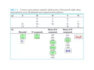
Introduction GaNZnO Bandgap (eV)3.43.3 µe (cm2/V-sec)220200 µh (cm2/V-sec)105-50 me0.27mo0.24mo mh0.8mo0.59mo Exciton binding28 60 energy (meV) • Direct, wide bandgap • Bulk ZnO (n-type) commercially available • Grown on inexpensive substrates at low temperatures • High exciton binding energy • Heterojunction by substitution in Zn-site • Cd ~ 3.0 eV • Mg ~ 4.0 eV • Nanostructures demonstrated • Ferromagnetism at practical Tc when doped with transition metals • Obstacle: good quality, reproducible p-type Potential Applications UV/Blue optoelectronics Transparent transistors Nanoscale detectors Spintronic devices
ICP Etching • Wet etching • HCl, HNO3, NH4Cl, and HF • Generally isotropic with limited resolution and selectivity • High-density plasma etching • Anisotropic with high resolution • Favored by modern manufacturing environment • Bulk, wurtzite (0001) ZnO from Eagle-Picher • Gas chemistry: • Cl2/Ar (10/5 sccm) & CH4/H2/Ar (3/8/5 sccm) • Constant ICP source power at 500W and process pressure at 1 mTorr • Varied rf chuck power: 50 – 300W
ICP Etching - Etch Rates CH4/H2/Ar ~3000 Å/min Cl2/Ar ~1200 Å/min
ICP Etching - Etch Mechanism Ion-Assisted Etch Mechanism ER E0.5-ETH0.5 ETH ~ 96 eV for CH4/H2/Ar Vapor pressure of etch products: (CH4)2Zn 301 mTorr at 20°C ZnCl2 1 mTorr at 428 °C
ICP Etching - Photoluminescence Optical degradation even at the lowest rf power
ICP - AFM Control 100 W rf 50 W rf 200 W rf 300 W rf Zn and O etch products removed at same rate
ICP Etching - AES and SEM Control O Zn CH4/H2/Ar 200W rf O Zn
ICP Etching - Summary • Dry etching is possible with practical etch rates using CH4/H2/Ar • Surface is smooth and stoichiometric • Anisotropic sidewalls • Optical quality is sensitive to ion energy and flux
Hydrogen in ZnO • Hydrogen • Predicted role as shallow donor • Introduced from growth ambient • Present in optimal plasma etch chemistry • Understand diffusion behavior and thermal stability • Bulk, wurtzite (0001) ZnO, undoped (n~1017cm-3) from Eagle-Picher • Hydrogen incorporation • Ion Implantation of 2H or 1H (100keV, 1015 - 1016 cm-2) • 2H plasma exposure in PECVD at 100-300°C, 30 mins • Post-annealing: 500 - 700°C
Hydrogen in ZnO - Implanted - SIMS Removal of 2H below SIMS limit at 700°C Thermally less stable than GaN (>900ºC)
Hydrogen in ZnO - Implanted - RBS/C Minimal affect on BS yield near surface Small increase in scattering peak (6.5% of the random level before implantation and 7.8% after implantation) the nuclear energy loss profile of 100keV H+ is max
Hydrogen in ZnO - Implanted - PL Severe optical degradation even after 700ºC anneal Point defect recombination centers dominate
Hydrogen in ZnO - Plasma - SIMS Large diffusion depth 2H diffuses as an interstitial, with little trapping by the lattice elements or by defects or impurities
Hydrogen in ZnO - Plasma/annealed - SIMS 2H completely evolve out of the crystal at 500°C
Hydrogen in ZnO - Plasma - CV • Effects 2H plasma treatment • Passivate the compensating acceptor impurities • Induces a donor state and increases the free electron concentration Suggest H from growth process n-type conductivity probably arises from multiple impurity sources
Hydrogen in ZnO Implanted Plasma exposure Implanted 2H is slightly more thermally stable: trapping at residual damage in the ZnO by the nuclear stopping process
Hydrogen in ZnO - Summary • Thermal stability and diffusion behavior of hydrogen in ZnO • T 700 °C completely evolved the implanted H from ZnO • Residual implant-induced defects severely degrade optical properties and minimal affect crystal structure • Plasma: incorporation depths of about 30 m for 0.5 hr at 300°C • T 500 °C to remove H introduced by plasma exposure • Thermal stability of the hydrogen retention : • direct implantation > plasma exposure • Trapping at residual implant damage
Ohmic Contacts • Require low specific contact resistance • Surface treatments • As-received • Organic solvents (trichloroethylene, methanol, acetone, 3 mins each) • H plasma • Ti/Al/Pt/Au metal scheme on n-type ZnO • Bulk • PLD films • Au/Ni/Au and Au on p-type ZnMgO
Ohmic Contacts - Ti/Al/Pt/Au on Bulk Cross-sectional view of circular TLM Metals RO R1 Bulk n-ZnO C = RS LT2 Marlow and Das, Solid-State Electron. 25 91 (1982) ρc lowest at 250 °C anneal ρc ~ 610-4 cm2 Severe contact degradation after 600 °C anneal
Ohmic Contacts - Growth: n-type ZnO:P Films Hall Hall Post-growth Post-growth Carrier conc Carrier conc mobility mobility Resistivity Resistivity Anneal T Anneal T 3 3 2 2 W W (°C) (°C) (#/cm (#/cm ) ) ( ( cm) cm) (cm (cm /Vs) /Vs) 20 20 ´ ´ 1.5 1.5 10 10 30 30 0.002 0.002 18.5 18.5 19 19 ´ ´ 6 10 6 10 425 425 0.013 0.013 7.8 7.8 18 18 ´ ´ 2.4 2.4 10 10 450 450 1.3 1.3 1.9 1.9 17 17 ´ ´ 3.2 3.2 10 10 500 500 12.8 12.8 1.5 1.5 15 15 ´ ´ 7.5 7.5 10 10 600 600 463 463 1.8 1.8 • N-type phosphorus-doped ZnO film on (0001) Al2O3 grown by PLD • Post-growth annealing • Increase anneal temperature • Decrease carrier concentration and Hall mobility • Increase resistivity • Reduction of shallow state density • P dopants activation as acceptors in O site Heo et al APL 83 1128 (2003)
Ohmic Contacts - Ti/Al/Pt/Au ZnO:P Films Ti/Al/Pt/Au (200/800/400/800)Å on PLD ZnO:P films Nonalloyed: n = 1.5 1020 cm-3 c = 8.7 10-7 -cm2 Annealed: Measured at RT: n = 6.0 1019 cm-3 c = 3.9 10-7 -cm2 Measured at 200 °C n = 2.4 1018 cm-3 c = 2.2 10-8 -cm2
Ohmic Contacts - p-type ZnMgO Films • Ohmic behavior after annealing 500 °C • Ti/Au more thermally stable than Ni/Au contacts • Severe degradation of Ni/Au after 600 °C anneal S. Kim et al APL 84 1904 (2004)
Ohmic Contacts - p-type ZnMgO Films Specific contact resistance after 600 °C anneal Au: 2.5 10-5 cm2 Au/Ni/Au: 7.6 10-6 cm2
Ohmic Contacts - Summary • Ti/Al/Pt/Au to n-type ZnO (bulk, thin film) • No significant improvement from H2 plasma treatment or organic solvent cleaning • AES revealed Ti-O interfacial reactions and intermixing between Al and Pt layers T250°C • Au/Ni/Au to p-type ZnMgO: lower C than Au alone
Schottky Contacts Previous Works • Metals: Au, Ag, Pd • Schottky barriers heights ~ 0.6-0.8 eV • Barrier heights not following the difference in the work function value interface defect states determine contact characteristics • Au is unstable even at 60°C This Work • Investigate the effect of UV surface cleaning • Metal schemes: • PLD n-type film: Pt • Bulk: Pt, W, W2B, W2B5, CrB2
Schottky Contacts - Pt/Au on Bulk • No ozone treatment: Linear I-V • Ozone treatment: • B = 0.696 eV • = 1.49 • Js = 6.17 10-6 A-cm-2
Schottky Contacts - UV Ozone - AFM No Ozone Treatment 30 min Ozone Treatment
Schottky Contacts - UV Ozone - XPS Desorption of surface C contaminants
Schottky Contacts - W/Pt/Au on Bulk Sputter-induced damages • Non-rectifying for 250 °C and 500 °C anneal • Rectifying after 700 °C anneal
Schottky Contacts - W/Pt/Au - AES • Post-deposition annealing 500 °C: no detectable intermixing • 700 C anneal: Zn diffused out to the Au-Pt interface, independent of whether the samples had been exposed to ozone
Schottky Contacts - W2B5 vs. W2B W2B5/Pt/Au as deposited W2B/Pt/Au as deposited W2B5/Pt/Au 600ºC annealed W2B/Pt/Au 600ºC annealed
Schottky Contacts - Summary • Ozone treatment removes surface C contamination • Pt contacts: ozone treatment produces transition from ohmic to rectifying behavior • W contacts: require annealing T 700°C to repair sputter-induced damages • AES revealed intermixing of metal layers and out-diffusion of Zn to Au-Pt interface • Low barrier heights for boride contacts • W2B showed good thermal stability high temperature ohmic contacts
p-n Junction Diode - Growth and Structure Circular ohmic contact (50 to 375 m diameter) Zn0.9Mg0.1O: P0.02 PLD film (~1.4 m) Buffer n-ZnO PLD film (~0.8 m) Bulk ZnO (0.5 mm, n ~ 1017 cm-3) Full backside ohmic contact • Pulsed laser deposition (PLD) • (0001) bulk ZnOsubstrate • Zn0.9Mg0.01O:P0.02 target • KrF excimer laser ablation source • Laser repetition rate: 1 Hz • Laser pulse energy density: 3 J-cm-2 • Growth: 400 °C, O2 overpressure of 20 mTorr Undoped buffer layer necessary for good rectifying behavior • Ohmic contacts: • p-ZnMgO: Pt/Au (200/800Å) • n-ZnO: Ti/Al/Pt/Au 200/400/200/800Å) • Annealed at 200 °C, 1 min, N2 ambient
p-n Junction Diode - IV Characteristics Measured at room temp: VRB –9.0 V Js 4.610-9 A·cm-2 Vf 4.0 V RON 14.5 m ·cm-2
p-n Junction Diode - Reverse Breakdown Temperature coefficient: Slightly negative ~ .1 to .2 V/K Presence of defects Non-optimized growth and processing
p-n Junction Diode - Summary • Demonstrated ZnO-based p-n junctions • ZnMgO/ZnO heterostructure system • n-type ZnO buffer on the ZnO substrate is critical in achieving acceptable rectification in the junctions • Important step in realizing minority carrier devices in the ZnO system
Conclusions • ICP etching • Methane-based chemistry • Practical etch rate but optical degradation • H in ZnO • Much less thermally stable than GaN • Completely evolve out by 700°C anneals • Ohmic contacts to ZnO • Straightforward n-type • Rapidly improving for p-type • Schottky contacts to ZnO • Low B for both n-type and p-type • Surface states dominate transport mechanism • p-n junction diode using ZnMgO/ZnO demonstrated
Acknowledgements • Committee members: • Prof. Stephen Pearton, Chair • Prof. Cammy Abernathy • Prof. David Norton • Prof. Rajiv Singh • Prof. Fan Ren, External • Contributors: