Download
1 / 1
10 likes | 209 Vues
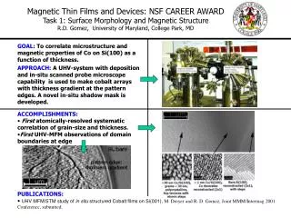
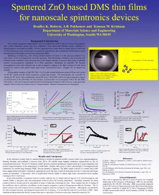
Figure 1) Picture of RF magnetron sputtering chamber in sputter down configuration. Plasma is purple with target just above brightest point, substrate is on flat section at bottom.

E N D
Figure 1) Picture of RF magnetron sputtering chamber in sputter down configuration. Plasma is purple with target just above brightest point, substrate is on flat section at bottom. Figure 4) Zero Field Cooled-Field Cooled magnetization measurements at H = 20 Oe. (a, b) with higher Co concentrations are granular multilayers showing blocking and superparamagnetism. (d) DMS with lowest relative Co concentration retains magnetization above 300K Figure 5) (ZnO20ÅCo2Å)25 hysteretic at 10 K & 300 K, background signal has been subtracted. Other samples showed superparamagnetism above their respective blocking temperatures. Figure 2) XRD Pattern of nano-crystalline ZnO with no metallic Co peaks visible; greater concentrations show diffuse metallic Co peaks Figure 3) Fitting toVariable Range Hopping law with n = ½. Equipment sensitivity reached a limit at high resistivity. Sputtered ZnO based DMS thin films for nanoscale spintronics devices Bradley K. Roberts, A.B. Pakhomov and Kannan M. KrishnanDepartment of Materials Science and EngineeringUniversity of Washington, Seattle WA 98195 Background & Introduction The wurtzite transparent semiconductor ZnO was predicted by Dietl et al.[1] to become ferromagnetic with a Curie temperature greater than room temperature when doped with transition metals, resulting in a diluted magnetic semiconductor (DMS). We have approached this system from two fronts and have found that Co /ZnO multilayers at the correct ratios of nominal layer thicknesses, and co-sputtered Cr:ZnO films at certain concentrations of the dopant are both room temperature DMSs. Multilayers of (ZnOxCoy)n, with varying nominal thickness of metal y=2-10Å and semiconductor x=2-20Å, and n= 25-50 were prepared by ion beam sputtering. With decreasing Co thickness and increasing ZnO thickness in the multilayer stack, the properties of the samples undergo a crossover from those of granular metallic Co/semiconductor multilayers to a DMS superlattice, determined by solubility. We interpret ferromagnetism in the latter (diluted) case as due to magnetic ordering in the high resistance Co-rich layers mediated by carriers from lightly doped, high carrier concentration layers. Roughly 5% Al dopant was included. Polycrystalline samples of ZnO:TM (TM = Co, Cr) with nominal thicknesses around 120 nm were grown via the DC (metal) and RF (ZnO) magnetron co-sputtering method. TM concentration was controlled by varying the DC power while maintaining constant RF power. Both XRD results and optical properties suggest Co incorporation in the ZnO lattice for most samples. Cr-doped films are ferromagnetic both at 5K and 300K. This system is only now being developed but shows promising initial magnetic data. However, a spin glass-type magnetic behavior has been found so far in Co-doped samples. Transport measurements are in progress. Ferromagnetic Paramagnetic or frozen spin glass Granular superparamagnetic or blocked Figure 9) Spin glass-type state in ZnO:Co cosputtered sample (15W Co deposition) at 5K, and low field loop (with no hysteresis) of sample at 300K Figure 7) ZnO 50W Cr 20W on Si showing clear hysteresis loops at 5 & 300K, background signal of the diamagnetic substrate subtracted. Figure 8) ZFC-FC of ZnO:Co cosputtered sample with freezing orblocking temperature of ~60K Figure 6) ZFC-FC magnetization of ZnO:Cr (20W Cr) with consistent magnetization up to room temperature Results and Conclusions In the multilayer system, high Co nominal thickness resulted in granular metallic systems which were superparamagnetic, showing blocking, and exhibited a crossover from 2D to 3D variable range hopping conduction characteristics as the Co concentration decreased. The low Co thickness sample showed consistent spontaneous magnetization up to room temperature and positive magnetoresistance at low temperatures in small fields. Samples with excess Co show reduced high-T ferromagnetism and conduction via variable range hopping (VRH) between granules is apparent. The DMS sample with low Co content shows both better magnetization and higher conductivity (qualitatively much like that of ZnO:Al) indicating that the Co moments and charge carriers are dependent. A “proximity” effect is hypothesized whereby lightly Co doped, high carrier concentration layers mediate exchange in the Co-rich layers. In the polycrystalline co-sputtered systems recently explored, the Co doped material appears to be non-ferromagnetic and instead exhibits a spin-glass state and paramagnetic behavior above the freezing temperature. Annealing treatments are being conducted both in vacuum and in O2 atmosphere in hopes of inducing a ferromagnetic state. These samples lack the Al doping of the multilayers which could have an influence on the magnetic properties, a point of disagreement within the literature. The Cr doped system on the other hand has shown exemplary magnetic properties at high Cr concentrations. Although the concentrations are only estimated currently, and transport measurements are in progress, it is seen that this material is most likely a DMS. Band calculations had predicted the ZnO:Cr system behaving as a spin-glass [2] and our results may change this opinion [3,4]. References [1] Dietl, T., Ohno, H., Matsukura, F., Cibert, J., & Ferrand, D. (2000) Science, 287(5455), 1019-22. [2] Sato, K., & Katayama-Yoshida, H. (2002) Semicond. Sci. Technol., 17(4), 367-76. [3] A.B. Pakhomov, B.K. Roberts, & Kannan M. Krishnan, Appl. Phys. Lett. Submitted, (2003). [4] A.B. Pakhomov, B.K. Roberts, & Kannan M. Krishnan, J. Appl. Phys. InPreparation, (2004). Acknowledgements This work is supported by NSF/ECS -0224138 and by the Campbell Endowment at the University of Washington. ABP was also partially supported by the UW/JIN fellowship. BKR was partially supported by the UW Center for Nanotechnology Early Bird Fellowship Award. The authors would like to thank Dr. S. Theva Thevuthasan of PNNL for RBS measurements and Dr. Scott Chambers of PNNL for helpful conversations.