Week Four
In this presentation, we will explore the design and simulation of various logic modules, reviewing the tiny example from last week while focusing on detailed static timing reports with added constraints. We will conduct brute force simulations and apply these concepts to a shift register. Additionally, the session will cover examples of module combinations and a detailed analysis of the Honkin’ Shifter. We will examine Verilog code and schematic modules, and review the waveforms generated during functional and timing simulations to highlight potential routing delays.

Week Four
E N D
Presentation Transcript
Week Four Design & Simulation Example slides
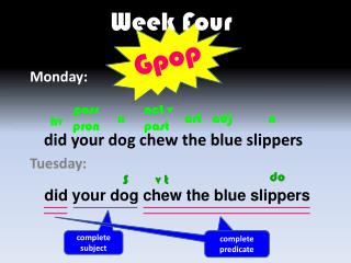
Agenda • Review the tiny example (Minako “logic”)from last week • look at the detailed static timing report with a constraint added in • Brute force a simulation • Do the same for a shift register • Give example of combining modules and do the same (MIX) • Look at Honkin’ Shifter Experiment
Logic: Code and Schematic module Logic( input A, input B, input C, input D, output OUT ); assign OUT = A & B | C & D; endmodule
Logic.ucf NET "A" LOC= P86; NET "B" LOC = P87; NET "C" LOC = P11; NET "D" LOC = P12; NET "OUT" LOC = P43; TIMESPEC TS1 = FROM:PADS(A):TO:PADS(OUT):9; TIMESPEC TS2 = FROM:PADS(B):TO:PADS(OUT):9; TIMESPEC TS3 = FROM:PADS(C):TO:PADS(OUT):9; TIMESPEC TS4 = FROM:PADS(D):TO:PADS(OUT):9;
module LogicTestbench; // Inputs reg A; reg B; reg C; reg D; // Outputs wire OUT; // Instantiate the Unit Under Test(UUT) Logic uut ( .A(A), .B(B), .C(C), .D(D), .OUT(OUT) ); initial begin // Initialize Inputs A = 0; B = 0; C = 0; D = 0; // Wait 100 ns for global reset to finish #100; // Add stimulus here A=1; B=1; C=0; D=0; // Wait 100 nsec for delay #100 A=0; B=0; C=0; D=0; // Wait 100 nsec for delay #100 A=0; B=0; C=1; D=1; //wait 100 nsec for delay #100 A=0; (ETC.)
Logic Waveforms(timing Sim) Note time delay due to routing delays
module Shifter( output reg DO, input [7:0] DI, input CLOCK, input RESET, input LOAD ); parameter piso_shift = 8; reg [piso_shift-2:0] DI_REG; //reg DO; always @(posedge CLOCK) if (RESET) begin DI_REG <= 0; DO <=0; end else if (LOAD) begin DI_REG <= DI[piso_shift-1:1]; DO <= DI[0]; end else begin DI_REG <= {1'b0, DI_REG[piso_shift-2:1]}; DO <= DI_REG[0]; end endmodule Shifter Verilog & RTL Schematic
Shifter: Simulation File `timescale 1ns/1ps module ShifterTBW; wire DO; reg [7:0] DI = 8'b00000000; reg CLOCK = 1'b0; reg RESET = 1'b0; reg LOAD = 1'b0; parameter PERIOD = 40; parameter real DUTY_CYCLE = 0.5; parameter OFFSET = 100; initial // Clock process for CLOCK begin #OFFSET; forever begin CLOCK = 1'b0; #(PERIOD-(PERIOD*DUTY_CYCLE)) CLOCK = 1'b1; #(PERIOD*DUTY_CYCLE); end end
Shifter UUT ( .DO(DO), .DI(DI), .CLOCK(CLOCK), .RESET(RESET), .LOAD(LOAD)); initial begin // ------------- Current Time: 105ns #105; RESET = 1'b1; DI = 8'b10101010; // ------------- Current Time: 145ns #40; RESET = 1'b0; // ------------- Current Time: 185ns #40; LOAD = 1'b1; // ------------- Current Time: 225ns #40; LOAD = 1'b0; // ------------------------------------- end endmodule
Mix: 8 Bit Register module register(C,D,CLR,Q); input C,CLR; input [7:0] D; output [7:0] Q; reg [7:0] Q; always @ (posedge C or posedge CLR) begin if (CLR) Q<= 8'b00000000; else Q<=D; end endmodule
Dual 8 Input, 8 Output Mux module octal_mux(INA,INB,OUT,SEL); input [7:0]INA; input [7:0]INB; output [7:0]OUT; input SEL; assign OUT [0] = (~SEL&INA[0]) | (SEL&INB[0]); assign OUT [1] = (~SEL&INA[1]) | (SEL&INB[1]); assign OUT [2] = (~SEL&INA[2]) | (SEL&INB[2]); assign OUT [3] = (~SEL&INA[3]) | (SEL&INB[3]); assign OUT [4] = (~SEL&INA[4]) | (SEL&INB[4]); assign OUT [5] = (~SEL&INA[5]) | (SEL&INB[5]); assign OUT [6] = (~SEL&INA[6]) | (SEL&INB[6]); assign OUT [7] = (~SEL&INA[7]) | (SEL&INB[7]); endmodule
Mix: Bolting them Together module MIX (CLOCK1,CLOCK2,CLEAR,SELECT,INPUTA,INPUTB,OUTPUT); input [7:0]INPUTA; input [7:0]INPUTB; output [7:0]OUTPUT; input SELECT; input CLOCK1; input CLOCK2; input CLEAR; wire [7:0]INA; wire [7:0]INB ; register copy1 (CLOCK1,INPUTA,CLEAR,INA); register copy2 (CLOCK2,INPUTB,CLEAR,INB); octal_mux copy3 (INA,INB,OUTPUT,SELECT); endmodule
Mix: Simulation File module Mix_tb; reg CLOCK1 = 1'b0; reg CLOCK2 = 1'b0; reg CLEAR = 1'b0; reg SELECT = 1'b0; reg [7:0] INPUTA = 8'b00000000; reg [7:0] INPUTB = 8'b00000000; wire [7:0] OUTPUT; parameter PERIOD = 100; parameter real DUTY_CYCLE = 0.5; parameter OFFSET = 100; initial // Clock process for CLOCK1 begin #OFFSET; forever begin CLOCK1 = 1'b0; #(PERIOD-(PERIOD*DUTY_CYCLE)) CLOCK1 = 1'b1; #(PERIOD*DUTY_CYCLE); end
MIX UUT ( .CLOCK1(CLOCK1), .CLOCK2(CLOCK2), .CLEAR(CLEAR), .SELECT(SELECT), .INPUTA(INPUTA), .INPUTB(INPUTB), .OUTPUT(OUTPUT)); initial begin // Process for CLOCK1 // ------------- Current Time: 100ns #100; INPUTA = 8'b00001010; // ------------------------------------- // ------------- Current Time: 135ns #35; CLEAR = 1'b1; INPUTA = 8'b00000101; // ------------------------------------- // ------------- Current Time: 235ns #100; CLEAR = 1'b0; INPUTA = 8'b00001010; INPUTB = 8'b00001111;
// ------------------------------------- // ------------- Current Time: 335ns #100; CLOCK2 = 1'b1; INPUTA = 8'b00000101; INPUTB = 8'b00000000; // ------------------------------------- // ------------- Current Time: 435ns #100; INPUTA = 8'b00001010; INPUTB = 8'b00001111; // ------------------------------------- // ------------- Current Time: 535ns #100; CLOCK2 = 1'b0; SELECT = 1'b1; INPUTA = 8'b00000101; INPUTB = 8'b00000000;
// ------------------------------------- // ------------- Current Time: 635ns #100; INPUTA = 8'b00001010; INPUTB = 8'b00001111; // ------------------------------------- // ------------- Current Time: 735ns #100; CLOCK2 = 1'b1; INPUTA = 8'b00000101; INPUTB = 8'b00000000; // ------------------------------------- // ------------- Current Time: 835ns #100; INPUTB = 8'b00001111; // ------------------------------------- // ------------- Current Time: 935ns #100; CLOCK2 = 1'b0; // ------------------------------------- end