Download
1 / 4
40 likes | 87 Vues
the first stage of each microwave receiver there is low noise amplifier LNA circuit, and this state has important rule in quality factor of the receiver. In this study, design and simulation of 15 GHz low noise amplifier LNA have been explored. This simulation has been performed by using the Agilent Advanced Design System ADS software. It also describes the design and simulation of a high frequency low noise amplifier, with high gain and low noise using MESFET for frequency 15GHz .A single stage LNA has successfully designed with 14.5 dB forward gain and 0.003dB noise figure in frequency of 15GHz.The NE76000 transistor was chosen for the design of the LNA due to its low noise figure, stability, and good gain at high frequency, good input and output impedance matching. Also the designed LNA should be working stably in frequency of 15GHz. Htun Myint "Design and Simulation of Low Noise Amplifier at 15 GHz Using Advanced Design System (ADS)" Published in International Journal of Trend in Scientific Research and Development (ijtsrd), ISSN: 2456-6470, Volume-2 | Issue-6 , October 2018, URL: https://www.ijtsrd.com/papers/ijtsrd18381.pdf Paper URL: http://www.ijtsrd.com/engineering/electronics-and-communication-engineering/18381/design-and-simulation-of-low-noise-amplifier-at-15-ghz-using-advanced-design-system-ads/htun-myint<br>

E N D
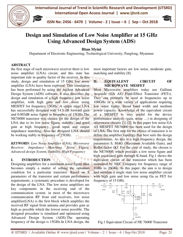
International Journal of Trend in International Open Access Journal International Open Access Journal | www.ijtsrd.com International Journal of Trend in Scientific Research and Development (IJTSRD) Research and Development (IJTSRD) www.ijtsrd.com ISSN No: 2456 ISSN No: 2456 - 6470 | Volume - 2 | Issue – 6 | Sep | Sep – Oct 2018 Design and Simulation of Low Using Advanced Design Syst Advanced Design System (ADS) Design and Simulation of Low Noise Amplifier at 15 GHz Noise Amplifier at 15 GHz Htun Myint Department of Electronic Enginee Electronic Engineering, Technological University, Panglong long, Myanmar ABSTRACT the first stage of each microwave receiver there is low noise amplifier (LNA) circuit, and this state has important rule in quality factor of the receiver. In this study, design and simulation of 15 GHz low noise amplifier (LNA) have been explored. This simul has been performed by using the Agilent Advanced Design System (ADS) software. It also describes the design and simulation of a high frequency low noise amplifier, with high gain and low noise using MESFET for frequency 15GHz .A single stage LNA has successfully designed with 14.5 dB forward gain and 0.003dB noise figure in frequency of 15GHz.The NE76000 transistor was chosen for the design of the LNA due to its low noise figure, stability, and good gain at high frequency, good input and output impedance matching. Also the designed LNA should be working stably in frequency of 15GHz. KEYWORD: Low Noise Amplifier (LNA), Microwave Receiver, Impedance Matching, Noise Figure, Advanced design System, Stability, High Frequency I. INTRODUCTION Designing amplifiers for a minimum noise figure then becomes simply a matter of setting the optimum condition for a particular transistor. Based on S parameters of the transistor and certain performance requirements, a systematic procedure is developed for the design of the LNA. The low noise key components in the receiving end of the communication system. in most of the microwave communication RF front end receivers, low noise amplifier(LNA) is the first block which amplifies the received RF signal from antenna and provides gain as high as possible which the lowest noise possible. The designed procedure is simulated and optimized using Advanced Design System (ADS).The operating frequency of the design is 15GHz.In LNA design most important factors are low noise, moderate g matching and stability [8]. II. EQUIVALENT MICROWAVE MESFET Most Microwave amplifiers today use Gallium Arsenide (GA AS) Field-Effect Transistor (FETs). They can presently be used at frequencies up to 100GHz in a wide variety of applications requiring low noise figure, broad band width and medium power capacity. Knowledge of the equivalent circuit of a MESFET is very useful for the device performance analysis (gain, noise …) in microwave circuits [1] [2]. In this paper low noise GA AS MESFET NE76000 has been used for the design of LNA. The first step for the choice of transistor is to define the amplifier topology that best suits the design requirements. As this is a high frequency design, the parameters S, MAG (Maximum Available Gain) Rollet factor (K). For the case of the NE76000, which provides a low noise figure and high associated gain through K equivalent circuit of the transistor which has been recovered by NEC Company for frequency range of 1GHz to 26GHz. In this paper; and simulate a single state low noise amplifier circuit with high gain and low noise using Ga frequency of 15 GHz. first stage of each microwave receiver there is low noise amplifier (LNA) circuit, and this state has important rule in quality factor of the receiver. In this study, design and simulation of 15 GHz low noise amplifier (LNA) have been explored. This simulation has been performed by using the Agilent Advanced Design System (ADS) software. It also describes the design and simulation of a high frequency low noise amplifier, with high gain and low noise using MESFET for frequency 15GHz .A single stage LNA successfully designed with 14.5 dB forward gain and 0.003dB noise figure in frequency of 15GHz.The NE76000 transistor was chosen for the design of the LNA due to its low noise figure, stability, and good gain at high frequency, good input and output nce matching. Also the designed LNA should be working stably in frequency of 15GHz. ant factors are low noise, moderate gain, EQUIVALENT MICROWAVE MESFET Most Microwave amplifiers today use Gallium CIRCUIT CIRCUIT OF OF Effect Transistor (FETs). They can presently be used at frequencies up to 100GHz in a wide variety of applications requiring low noise figure, broad band width and medium power capacity. Knowledge of the equivalent circuit of a MESFET is very useful for the device noise …) in designing of [2]. In this paper low noise GA AS MESFET NE76000 has been used for the design of LNA. The first step for the choice of transistor is to define the amplifier topology that best suits the design uirements. As this is a high frequency design, the parameters S, MAG (Maximum Available Gain), and For the case of study, the chosen is provides a low noise figure and high associated gain through K-band. Fig.1 shows the equivalent circuit of the transistor which has been recovered by NEC Company for frequency range of paper; the aim is to design and simulate a single state low noise amplifier circuit high gain and low noise using Ga as FET for Low Noise Amplifier (LNA), Microwave Receiver, Impedance Matching, Noise Figure, High Frequency Designing amplifiers for a minimum noise figure then becomes simply a matter of setting the optimum condition for a particular transistor. Based on S parameters of the transistor and certain performance requirements, a systematic procedure is developed for amplifiers are key components in the receiving end of the in most of the microwave communication RF front end receivers, low noise amplifier(LNA) is the first block which amplifies the signal from antenna and provides gain as high as possible which the lowest noise possible. The designed procedure is simulated and optimized using Advanced Design System (ADS).The operating In LNA design, the Fig.1 Equivalent Circuit of NE 76000 Transistor Fig.1 Equivalent Circuit of NE 76000 Transistor @ IJTSRD | Available Online @ www.ijtsrd.com www.ijtsrd.com | Volume – 2 | Issue – 6 | Sep-Oct 2018 Page: 21
International Journal of Trend in Scientific Research and Development (IJTSRD) ISSN: 2456 International Journal of Trend in Scientific Research and Development (IJTSRD) ISSN: 2456 International Journal of Trend in Scientific Research and Development (IJTSRD) ISSN: 2456-6470 III. DC BIASING Table.1 LNA Requirements Parameters Operating frequency Bias Point Technology Gain Noise Figure Then the overall transducer gain is GT=G The effective gains from GS and GL are due to the impedance matching of the transistor to the impedance Z0. Then the overall transducer gain is GT=GS’GoGL. The effective gains from GS and GL are due to the impedance matching of the transistor to the Table.1 LNA Requirements specification 15GHz Vd=3v,Ids=10mA Ga As MESFET >14.4 <1 <1 cification 15GHz Vd=3v,Ids=10mA As MESFET >14.4 Fig.2 the General Transistor Amplifier Circuit General Transistor Amplifier Circuit In order to design a low noise device, the transistor must be DC biased at an appropriate operating point. These depends of the application (low noise gain, high power), and the type of the transistor ( HFET, etc) [4]. The circuit is designed to meet the chosen biasing, considering that very high values of resistance naturally add more noise to the system, and very low resistance increase the power consumption of the system. Accounts both source and load mismatch. Thus from [6],can be separate effective gain factors for the input (source) matching network, the transistor itself and the output (load) matching network as follow. Vd (drain voltage) =3V and Ids (drain-Source current) =10mA.This biasing point is obtained by using a (gate voltage) range from -0.6 to 3 V [5]. A.Single Stage Amplifier A single stage amplifier microwave transistor amplifier can be modeled by the circuit in Fig.2, where a matching network is used both sides of the transistor to transform the input and output impedance Z0 to the source and load impedance Zs and ZL. The most useful gain definition for amplifier design is the transducer power gain, which accounts both source and load mismatch. Thus from[6], can be defined separate effective gain factors for the input (source) matching network, the transistor itself and output (load) matching network As follow: 2 ' 2 1 IN S −Γ Γ 2 1 L L L S − Γ B.Stability Consideration The stability of an amplifier oscillate, is a very important consideration in a design and can be determined from matching networks, and the terminations. circuit, oscillations are possible w or output port presents a negative resistance. occurs when IN Γ >1 or OUT Γ and OUT Γ depend on the source and load matching networks. While, the stability of the amplifier depends on S Γ and L Γ as presented by the matching networks, when starting on any amplifier design it is very important to spend time checking on the stability of the device chosen, otherwise the amplifier may well turn into an oscillator. The main way of determining the stability of a device is to calculate the Rollett’s stability factor(K), which is calculate using a set of S-parameters for the device at the frequency of operation. Alternatively, it can be shown that amplifier will be unconditionally stable if the following necessary and sufficient conditions are met [7]. 2 2 11 22 1 2 . S S 1 ∆ < K=1.393 C.Matching Network Design The need for matching network arises because amplifiers, in order to deliver maximum power to a load, or to perform in a certain desired way, must be properly terminated at both the input and outp Several types of matching network are available, however factors likes complexity, bandwidth implementation and adjustability need to be considered in the matching network seletion. The amplifier could be matched for a variety of conditions such as low noise applications, bilateral case. The impedance matching networks can be designed either mathematically or graphically. be designed either mathematically or graphically. In order to design a low noise device, the transistor operating point. The stability of an amplifier, or its resistance to very important consideration in a design and can be determined from the S parameters, the networks, and the terminations. In the oscillations are possible when either the input or output port presents a negative resistance. This application (low noise, high transistor (FET, The circuit is designed to meet the chosen biasing, considering that very high values of resistance naturally add more noise to the system, and very low esistance increase the power consumption of the system. Accounts both source and load mismatch. Thus from [6],can be separate effective gain factors for the input (source) matching network, the transistor itself and the output (load) matching network as Γ >1.These because of >1.These because of IN depend on the source and load matching the stability of the amplifier depends sented by the matching starting on any amplifier design it is o spend time checking on the stability of the device chosen, otherwise the amplifier may well turn into an oscillator. The main way of determining the stability of a device is to calculate the Source current) =10mA.This biasing point is obtained by using a Vg which is calculate using a 5]. parameters for the device at the frequency of operation. Alternatively, it can be shown that amplifier will be unconditionally stable if the following necessary and sufficient conditions are met single stage amplifier microwave transistor the circuit in Fig.2, where a matching network is used both sides of the transistor to transform the input and output impedance Z0 to the source and load impedance Zs and ZL. The most useful gain definition for amplifier design is the , which accounts both source 2 2 2 2 − − − − + ∆ + ∆ S S = = > > S (3) 1 K 21 12 can be defined Matching Network Design The need for matching network arises because amplifiers, in order to deliver maximum power to a load, or to perform in a certain desired way, must be properly terminated at both the input and output port. Several types of matching network are available, ors likes complexity, bandwidth, implementation and adjustability need to be considered in the matching network seletion. The amplifier could be matched for a variety of conditions as low noise applications, unilateral case and The impedance matching networks can separate effective gain factors for the input (source) matching network, the transistor itself and output − Γ 1 = S (1) G s − Γ = (2) G 2 1 22 @ IJTSRD | Available Online @ www.ijtsrd.com www.ijtsrd.com | Volume – 2 | Issue – 6 | Sep-Oct 2018 Page: 22
International Journal of Trend in Scientific Research and Development (IJTSRD) ISSN: 2456 International Journal of Trend in Scientific Research and Development (IJTSRD) ISSN: 2456 International Journal of Trend in Scientific Research and Development (IJTSRD) ISSN: 2456-6470 IV. NOISE RESULT NOISE FIGURES FIGURES SIMULATION SIMULATION The minimum noise figure is needed in order to achieve the maximum gain.Fig.3 Show the minimum noise figure plot. The Lowest Fm obtained at frequency 15GHz. The minimum noise figure is needed in order to gain.Fig.3 Show the minimum in 0.004 dB Fig.5 S12 Parameter Plot Parameter Plot Fig.3 Minimum Noise Figure Fig.3 Minimum Noise Figure V. The designed LNA with matching network at 15GHz was obtained. The forward gain (S21), isolation S11 and S22 plot is shown in figures. The results shows that the 11 S <1 and 22 S condition. The highest forward gain (S21)is 14.49dB at 15GHz as shown in Fig.6.The design LNA also isolation when S12 value is below -50dB at 15GHz. Also the stability factor, K=1.393 plot is shown in Fig.8.Thus the design LNA should be working stably in frequency of 15GHz. EXPERIMENTAL RESULT The designed LNA with matching network at 15GHz isolation (S12), The results shows Fig.6 S21 Parameter Plot Parameter Plot <1 full fills the stability fills the stability )is 14.49dB at 15GHz as shows a good 50dB at 15GHz. Also the stability factor, K=1.393 plot is shown in Fig.8.Thus the design LNA should be working stably Fig.7 S22 Parameter Plot Parameter Plot Fig.8 Stability Factor K Plot Factor K Plot Fig.4 S11 Parameter Plot @ IJTSRD | Available Online @ www.ijtsrd.com www.ijtsrd.com | Volume – 2 | Issue – 6 | Sep-Oct 2018 Page: 23
International Journal of Trend in Scientific Research and Development (IJTSRD) ISSN: 2456 International Journal of Trend in Scientific Research and Development (IJTSRD) ISSN: 2456 International Journal of Trend in Scientific Research and Development (IJTSRD) ISSN: 2456-6470 4.Microwave Engineering- Wiley &Sons. INC-New York Weinheim. Brisbane-Singapore. Toronto. 5.Agilent Technologies (2000).”Application 1190-Low Noise Amplifier for Agilent ATF-34143.Low Noise PHEMT”.USA: Agilent Technologies 1-8. 6.D.M Pozar (2000). ”Microwave RF Wireless System”, United State of America: and sons Inc 77797, 205-207. 7.Microwave Transistor Amplifi Design Guillermo Gonzalez Prentice-Hall, Inc Englewood Cliffs, 07632. 8.Mohd. Zinol Abidin Abd Aziz Amplifier Circuit Design for 5GHz to 6GHz”, Proceeding of the 2004 IEEE RF and microwave conference, Subang, Selangor, Malasia. Malaysia will be deleted from the biography. Malaysia will be deleted from the biography. VI. In this paper, LNA at 15 GHz for microwave receiver system have been designed and simulated. It is observed that the forward gain and noise figure of these designs is almost 14.49 dB and 0.004 dB respectively in 15GHz.This simulation result have good assent with desired demand. VII. REFERENCES 1.C.A BAL anis, Antenna Theory: Analysis and design, Harper and Row N. Y., 1982 2.K. Miyauchi, “Millimeter-Wave Communi “in Infrared and millimeter waves, Button, ED, Academic pres, N. Y., 1983 3.Exclusive North America Agent for NEC RF, Microwave &optoelectronic semiconductors CEL California Eastern Laboratories- 4590 Parick Heny Drive, Santa clora, CA 95054 1817-www.CEL.com. CONCLUSION In this paper, LNA at 15 GHz for microwave receiver system have been designed and simulated. It is observed that the forward gain and noise figure of designs is almost 14.49 dB and 0.004 dB respectively in 15GHz.This simulation result have -David M-Pozar. John New York. Chichester. Singapore. Toronto. Agilent Technologies (2000).”Application No to Low Noise Amplifier for 900MHz using the 34143.Low Noise PHEMT”.USA: ”Microwave RF Wireless United State of America: John Wiley 207. , Antenna Theory: Analysis and , 1982. Microwave Transistor Amplifier Analysis and Design Guillermo Gonzalez, Ph.D.1984 by Inc Englewood Cliffs, New Jersey Communication, Infrared and millimeter waves, vol. 9, K. J. , 1983. Exclusive North America Agent for NEC RF, Microwave &optoelectronic semiconductors CEL Zinol Abidin Abd Aziz (2004),”Low Noise Amplifier Circuit Design for 5GHz to 6GHz”, Proceeding of the 2004 IEEE-0-7083-8671-X/04/- crowave conference, October 5-6, Malasia. 81300skudia, Johor, -Headquarters- a clora, CA 95054- Fig.9 Input and Output Matching Network Of designed LNA Fig.9 Input and Output Matching Network Of designed LNA Fig.9 Input and Output Matching Network Of designed LNA @ IJTSRD | Available Online @ www.ijtsrd.com www.ijtsrd.com | Volume – 2 | Issue – 6 | Sep-Oct 2018 Page: 24