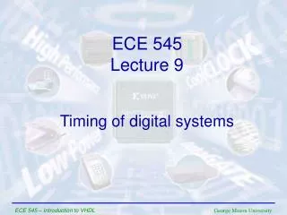
Timing of digital systems
540 likes | 742 Vues
ECE 545 Lecture 9. Timing of digital systems. What is an FPGA Chip ?. I/O Block. I/O Block. I/O Block. I/O Block. F ield P rogrammable G ate A rray A chip that can be configured by user to implement different digital hardware Configurable Logic Blocks and Programmable Switch Matrices

Timing of digital systems
E N D
Presentation Transcript
ECE 545 Lecture 9 Timing of digital systems ECE 545 – Introduction to VHDL
What is an FPGA Chip ? I/O Block I/O Block I/O Block I/O Block • Field Programmable Gate Array • A chip that can be configured by user to implement different digital hardware • Configurable Logic Blocks and Programmable Switch Matrices • Bitstream to configure: function of each block & the interconnection between logic blocks Source: [Brown99] ECE 545 – Introduction to VHDL
CLB Structure ECE 545 – Introduction to VHDL
CLB Slice COUT YB Carry & Control Logic Look-Up Table Y G4 G3 G2 G1 S D Q O CK EC R F5IN BY SR XB Look-Up Table Carry & Control Logic X S F4 F3 F2 F1 D Q O CK EC R CIN CLK CE SLICE ECE 545 – Introduction to VHDL
LUT (Look-Up Table) Functionality • Look-Up tables are primary elements for logic implementation • Each LUT can implement any function of 4 inputs ECE 545 – Introduction to VHDL
Design process (1) Specification Design and implement a simple unit permitting to speed up encryption with RC5-similar cipher with fixed key set on 8031 microcontroller. Unlike in the experiment 5, this time your unit has to be able to perform an encryption algorithm by itself, executing 32 rounds….. VHDL description (Your VHDL Source Files) Library IEEE; use ieee.std_logic_1164.all; use ieee.std_logic_unsigned.all; entity RC5_core is port( clock, reset, encr_decr: in std_logic; data_input: in std_logic_vector(31downto0); data_output: out std_logic_vector(31downto0); out_full: in std_logic; key_input: in std_logic_vector(31downto0); key_read: out std_logic; ); end AES_core; Functional simulation Synthesis Post-synthesis simulation ECE 545 – Introduction to VHDL
Design process (2) Implementation (Mapping, Placing & Routing) Timing simulation Configuration On chip testing ECE 545 – Introduction to VHDL
Design Process control from Active-HDL ECE 545 – Introduction to VHDL
Logic Synthesis VHDL description Circuit netlist architecture MLU_DATAFLOW of MLU is signal A1:STD_LOGIC; signal B1:STD_LOGIC; signal Y1:STD_LOGIC; signal MUX_0, MUX_1, MUX_2, MUX_3: STD_LOGIC; begin A1<=A when (NEG_A='0') else not A; B1<=B when (NEG_B='0') else not B; Y<=Y1 when (NEG_Y='0') else not Y1; MUX_0<=A1 and B1; MUX_1<=A1 or B1; MUX_2<=A1 xor B1; MUX_3<=A1 xnor B1; with (L1 & L0) select Y1<=MUX_0 when "00", MUX_1 when "01", MUX_2 when "10", MUX_3 when others; end MLU_DATAFLOW; ECE 545 – Introduction to VHDL
Synthesis Tools … and others ECE 545 – Introduction to VHDL
Features of synthesis tools • Interpret RTL code • Produce synthesized circuit netlist in a standard EDIF format • Give preliminary performance estimates • Some can display circuit schematics corresponding to EDIF netlist ECE 545 – Introduction to VHDL
Timing report after synthesis Performance Summary ******************* Worst slack in design: -0.924 Requested Estimated Requested Estimated Clock Clock Starting Clock Frequency Frequency Period Period Slack Type Group ------------------------------------------------------------------------------------------------------- exam1|clk 85.0 MHz 78.8 MHz 11.765 12.688 -0.924 inferred Inferred_clkgroup_0 System 85.0 MHz 86.4 MHz 11.765 11.572 0.193 system default_clkgroup =========================================================== ECE 545 – Introduction to VHDL
Implementation • After synthesis the entireimplementation process is performed by FPGA vendor tools ECE 545 – Introduction to VHDL
Mapping LUT0 LUT4 LUT1 FF1 LUT5 LUT2 FF2 LUT3 ECE 545 – Introduction to VHDL
Placing FPGA CLB SLICES ECE 545 – Introduction to VHDL
Routing FPGA Programmable Connections ECE 545 – Introduction to VHDL
Map report header Release 7.1.03i Map H.41 Xilinx Mapping Report File for Design 'exam1' Design Information ------------------ Command Line : c:\Xilinx\bin\nt\map.exe -p 2S200FG256-6 -o map.ncd -pr b -k 4 -cm area -c 100 -tx off exam1.ngd exam1.pcf Target Device : xc2s200 Target Package : fg256 Target Speed : -6 Mapper Version : spartan2 -- $Revision: 1.26.6.4 $ Mapped Date : Wed Nov 02 11:15:15 2005 ECE 545 – Introduction to VHDL
Map report Design Summary -------------- Number of errors: 0 Number of warnings: 0 Logic Utilization: Number of Slice Flip Flops: 144 out of 4,704 3% Number of 4 input LUTs: 173 out of 4,704 3% Logic Distribution: Number of occupied Slices: 145 out of 2,352 6% Number of Slices containing only related logic: 145 out of 145 100% Number of Slices containing unrelated logic: 0 out of 145 0% *See NOTES below for an explanation of the effects of unrelated logic Total Number 4 input LUTs: 210 out of 4,704 4% Number used as logic: 173 Number used as a route-thru: 5 Number used as 16x1 RAMs: 32 Number of bonded IOBs: 74 out of 176 42% Number of GCLKs: 1 out of 4 25% Number of GCLKIOBs: 1 out of 4 25 ECE 545 – Introduction to VHDL
Place & route report Timing Score: 0 Asterisk (*) preceding a constraint indicates it was not met. This may be due to a setup or hold violation. -------------------------------------------------------------------------------- Constraint | Requested | Actual | Logic | | | Levels -------------------------------------------------------------------------------- TS_clk = PERIOD TIMEGRP "clk" 11.765 ns | 11.765ns | 11.622ns | 13 HIGH 50% | | | -------------------------------------------------------------------------------- OFFSET = OUT 11.765 ns AFTER COMP "clk" | 11.765ns | 11.491ns | 1 -------------------------------------------------------------------------------- OFFSET = IN 11.765 ns BEFORE COMP "clk" | 11.765ns | 11.442ns | 2 -------------------------------------------------------------------------------- ECE 545 – Introduction to VHDL
Post layout timing report Timing summary: --------------- Timing errors: 0 Score: 0 Constraints cover 42912 paths, 0 nets, and 1038 connections Design statistics: Minimum period: 11.622ns (Maximum frequency: 86.044MHz) Minimum input required time before clock: 11.442ns Minimum output required time after clock: 11.491ns ECE 545 – Introduction to VHDL
Timing of digital circuits ECE 545 – Introduction to VHDL
Timing Characteristics of Combinational Circuits LUT LUT LUT tp LUT tp routing Total propagation delay through combinational logic • Combinational Circuits Are Characterized by Propagation Delays • through logic components (gates, LUTs) • through interconnects (routing delays) ECE 545 – Introduction to VHDL
Timing Characteristics of Combinational Circuits (2) • Total Propagation Delay of Logic Depends on the Number of Logic Levels and Delays of Logic Components • Number of logic levels is the number of logic components (gates, LUTs) the signal propagates through • Routing Delays Depend on: • Length of interconnects • Fanout ECE 545 – Introduction to VHDL
Timing Characteristics of Combinational Circuits (3) LUT LUT LUT LUT • Fanout – Number of Inputs Connected to One Output • Each inputs has its capacitance • Fast switching of outputs with high fanout requires higher currents and strong drivers ECE 545 – Introduction to VHDL
Timing Characteristics of Combinational Circuits (4) • In Current Technologies Routing Delays Make 50-70% of the Total Propagation Delays ECE 545 – Introduction to VHDL
Timing Characteristics of Sequential Circuits (1) • Timing Features of Flip-flops • Setup time tS – minimum time the input has to be stable before the rising edge of the clock • Hold time tH – minimum time the input has to be stable after the rising edge of the clock • Propagation delay tP – time to propagate input to output after the rising edge of the clock ECE 545 – Introduction to VHDL
Timing Characteristics of Sequential Circuits (2) clk clk D tS tH D Q Q tP Input D must remain stable during this interval Input D can freely change during this interval ECE 545 – Introduction to VHDL
Critical Path (1) out in clk D D Q Q • Critical Path – The Longest Path From Outputs of Registers to Inputs of Registers t logic tCritical = tFF-P + tlogic + tFF-setup ECE 545 – Introduction to VHDL
Critical Path (2) • Min. Clock Period = Length of The Critical Path • Max. Clock Frequency = 1 / Min. Clock Period ECE 545 – Introduction to VHDL
n+m n+m ECE 545 – Introduction to VHDL
Clock Jitter • Rising Edge of The Clock Does Not Occur Precisely Periodically • May cause faults in the circuit clk ECE 545 – Introduction to VHDL
Clock Skew out in clk delay out in D D Q Q D D Q Q clk delay • Rising Edge of the Clock Does Not Arrive at Clock Inputs of All Flip-flops at The Same Time ECE 545 – Introduction to VHDL
Clock skew ECE 545 – Introduction to VHDL
H-clock tree used to minimize clock skew ECE 545 – Introduction to VHDL
Dealing With Clock Problems • Use Only Dedicated Clock Nets for Clock Signals • Do Not Put Any Logic in Clock Nets ECE 545 – Introduction to VHDL
Basic I/O Block Structure Q D Three-State EC FF Enable Three-StateControl Clock SR Set/Reset Q D Output EC FF Enable Output Path SR Direct Input FF Enable Input Path Q D Registered Input EC SR ECE 545 – Introduction to VHDL
IOB Functionality • IOB provides interface between the package pins and CLBs • Each IOB can work as uni- or bi-directional I/O • Outputs can be forced into High Impedance • Inputs and outputs can be registered • advised for high-performance I/O • Inputs can be delayed ECE 545 – Introduction to VHDL
Timing simulation after implementation ECE 545 – Introduction to VHDL
Timing vs. functional simulation • Simulation before synthesis is used to verify circuit functionality and may differ from the one aftersynthesis and implementation • Implementation tool generates SDF (Standard Delay Format) as a standard delay file and thenetlist for synthesized VHDL code with delays. • Generated netlist contains many component instantiation statements with library references ECE 545 – Introduction to VHDL
SDF file A part of the SDF file is shown below. It indicates XOR gate delays (low to high, high to low) of minimum, typical and worst case timing ( DELAYFILE ( CELL( CELLTYPE “XOR”) ( INSTANCE U34.Z_VTX) ( DELAY( INCREMENT ( DEVICE 01 (0.385090:0.385090:0.385090)(0.235177: 0.235177: 0.235177) ) ) ) ) ECE 545 – Introduction to VHDL
Netlist from the synthesis tool U30 : MUX21L port map( Z => n71, A => n67, B => n68, S => n69); U31 : EN port map( Z => n67, A => D1, B => D0); U32 : IV port map( Z => n68, A => n67); U33 : EOP port map( Z => n69, A => D6, B => D7); U34 : EO3 port map( Z => n70, A => D3, B => D2, C => D4); U35 : EO port map( Z => n72, A => D5, B => n70); U36 : EOP port map( Z => XOR8, A => n72, B => n71); U37 : FA1A port map( S => n73, CO => n76, CI => D3, A => D2, B => FF); U38 : EO3 port map( Z => n74, A => n68, B => n73, C => D4); U39 : EOP port map( Z => FF_COMB_OUT, A => D5, B => n74); end structural; library IEEE; library TC200G; use IEEE.std_logic_1164.all; use TC200G.components.all; entity CONSYN is port( RSTn, CLK, D0, D1, D2, D3, D4, D5, D6, D7 : in std_logic; FF_OUT, COMB_OUT, FF_COMB_OUT : out std_logic); end CONSYN; architecture structural of CONSYN is signal XOR8, FF, n70, n71, n72, n73, n74, n75, n76, n67, n68, n69 : std_logic; begin FF_OUT <= FF; COMB_OUT <= XOR8; FF_reg : FD2 port map( Q => FF, QN => n75, D => XOR8, CP => CLK, CD => RSTn) ; ECE 545 – Introduction to VHDL
Timing parameters ECE 545 – Introduction to VHDL
Timing parameters units definition pipelining time pointpoint ns delay rising edge rising edge of clock ns good clock period 1 MHz clock frequency good clock period ns bad latency time inputoutput throughput Mbits/s good #output bits/time unit ECE 545 – Introduction to VHDL
Basic iterative architecture of the encryption/decryption unit multiplexer register combinational logic round keys one round enc_dec ECE 545 – Introduction to VHDL
Basic iterative architecture: Timing CLK M3 M1 M2 IN C1 C2 OUT Latency k · clock_period ECE 545 – Introduction to VHDL
Increasing throughput using pipelining round 1 Throughput = block size target clock period, e.g., 20 ns . . . target_clock_period round 16 ECE 545 – Introduction to VHDL
Optimizationcriteria ECE 545 – Introduction to VHDL
Degrees of freedom and possible trade-offs speed area power testability ECE 545 – Introduction to VHDL
Degrees of freedom and possible trade-offs speed latency area throughput ECE 545 – Introduction to VHDL