Download

1 / 24
240 likes | 431 Vues
Low Noise Charge Sensitive Preamplifier Development for the PANDA Calorimeter. Design and Measurements of the APFEL - Chip. Outline. PANDA – Experiment Overview Design of the APFEL – Chip Measurements of the ASIC – Performance. 1. The PANDA-Experiment. PANDA - Experiment. PANDA.

E N D
Low Noise Charge Sensitive Preamplifier Development for the PANDA Calorimeter Design and Measurements of the APFEL - Chip Peter, Wieczorek - EE
Outline • PANDA – Experiment Overview • Design of the APFEL – Chip • Measurements of the ASIC – Performance Peter, Wieczorek - EE
1. The PANDA-Experiment Peter, Wieczorek - EE
PANDA - Experiment PANDA Peter, Wieczorek - EE
Physical Goals • The aim of the PANDA – experiment is the better understanding of the strong interaction as well as the structure and dynamics of hadrons • Studies of bound quarks using meson spectroscopie • Bound qq – states • Theoretical description by QCD • Looking for exotic states • Hybrids (qqg) • Glueballs (ggg) • Molecule p Momentum [GeV/c] Molecules Gluons Mesons Mass [GeV/c2] Peter, Wieczorek - EE
Charmonium Spectra p Momentum [GeV/c] Mass [GeV/c2] • Charmonium: cc – quarks • Spectra of exicited states • Activation of all states by pp – interaction • Search of the theoretical predicted mesons Detection of charged and neutral particals over the whole solid angle Peter, Wieczorek - EE
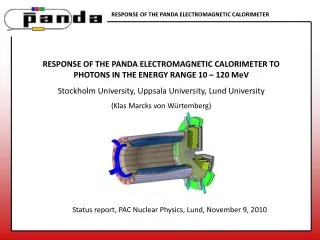
PANDA - Detector Target Solenoid Myondetector Dipol RICH p STT EMC HC EMC MVD STT DIRC Peter, Wieczorek - EE
Electromagnetic Calorimeter • Photon detection by the electromagnetic calorimeter • 11000 crystals (Barrel) • Used scintillator material: PbWO4 • To increase the crystal light yield the calorimeter will operate at a temperature of T = - 20°C Peter, Wieczorek - EE
Scintillator Material Output Voltage λmax = 430 nm • e- ….. Photon • e+ Scintillator Crystal Avalanche Photodiode Readout Electronics ? Peter, Wieczorek - EE
Requirements • Noise: ENC = 4500 e- ( ≈ 0,7 fC) • Max. input charge: Qmax = 7 pC • Dyn. range: 10000 • Event rate: ≈ 350 kHz • Avalanche photodiode: • Detector capacitance: Cdet = 300 pF • Dark current: Id = 50 nA at M = 50 • Operation Temperature: T = -20°C • Power dissipation: P < 60 mW/Channel • Very compact calorimeter design High integration level of the readout electronics Development of an application specific integrated circuit Peter, Wieczorek - EE
2. APFEL - Chip Design(Asic for Panda Frontend ELectronics) Peter, Wieczorek - EE
Noise Calculations W • Feasibility study for integrated calorimeter readout electronics • The dominant noise source is the input transistor • Transistor noise is a function of • Transistorwidth W • Current Ids • Integration time Signal Area ~ Noise • Ids Preselection of the free parameters: W = 12000 µm, Ids = 2 mA and = 250 ns Peter, Wieczorek - EE
Readout Concept • Readout is realized in three stages • First readout stage is a low noise Charge Sensitive Amplifier (CSA) based on a folded cascode circuit • Second stage consists of a differentiator and three first order integrators • Semi gaussian pulse form • Improvement of the Signal-to-Noise-Ratio (SNR) • The last stage is an output/line driver, which can cope with a load of 10 pF || 50 kΩ Peter, Wieczorek - EE
Concept of the Readout Electronic Shaper Stage Output Stage Charge Sensitive Amplifier - Preamp First Shaper Second Shaper Third Shaper Peter, Wieczorek - EE
Chip Overview Shaper Stage • Used prozess: 350 nm - CMOS • Dimensions: 3,3 mm x 3,3 mm • Pins: 64 • Components: • Transistors: 4841 • Capacitors: 1729 • Resistors: 386 Channel 1 Charge Sensitive Preamplifier Output Stage Channel 2 Voltage References Peter, Wieczorek - EE
3. Chip Characterisation Peter, Wieczorek - EE
PCB for the ASIC Characterisation • For the characterisation of the ASIC a PCB was designed • Power supply (Vddc,Vddt): 3.3 V • For measurements a voltage step ΔV injected to a coupling capacitance • With the voltage step ΔV and the capacitance Cin the injected input charge can be calculated to Qin = CinΔV Peter, Wieczorek - EE
Cooling Input Output • For cooling an external controlled Peltier-Element is used • Measurements in the range of T=-20°C up to T=+20°C could be realized • The current ASIC temperature is measured by a PT100 PT100 Cooper Peltier Element Peter, Wieczorek - EE
Measurement Setup (1) • Measurements are performed in an evacuated environment • Water cooling for heat sinking • Electrical connections are done via BNC - connectors Peter, Wieczorek - EE
Power Supply Signal Generator AWG Oscilloscope Programming PCB Temperature Controller Measurement Setup (2) • Defined input step ΔV by an AWG • Measuring the output pulse characteristics at • Different temperatures • Different detector capacitances Peter, Wieczorek - EE
Output Pulse • Amplitude & Rise time • Noise Peter, Wieczorek - EE
Measured Results Peter, Wieczorek - EE
Status • The developed APFEL- chip fulfills all requirements • First preliminary radiation tests have been done Next steps • More detailed radiation tests are necessary • Readout of an array of crystals Peter, Wieczorek - EE
Thank you for your attention Peter, Wieczorek - EE