Download
1 / 82
860 likes | 1.49k Vues
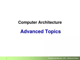
Computer Architecture & Related Topics. Ben Schrooten Shawn Borchardt, Eddie Willett Vandana Chopra. Computer Architecture History Single Cpu Design GPU Design (Brief) Memory Architecture. Communications Architecture Dual Processor Design Parallel & Supercomputing Design.

E N D
Computer Architecture& Related Topics Ben Schrooten Shawn Borchardt, Eddie Willett Vandana Chopra
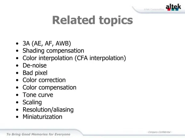
Computer Architecture History Single Cpu Design GPU Design (Brief) Memory Architecture Communications Architecture Dual Processor Design Parallel & Supercomputing Design PresentationTopics
Part 1 History and Single Cpu Ben Schrooten
HISTORY!!! One of the first computing devices to come about was . . The ABACUS!
The ENIAC : 1946 • Completed:1946 • Programmed:plug board and switches • Speed:5,000 operations per second • Input/output:cards, lights, switches, plugs • Floor space:1,000 square feet
The EDSAC(1949) and The UNIVAC I(1951) UNIVAC Speed:1,905 operations per second Input/output:magnetic tape, unityper, printer Memory size:1,000 12-digit words in delay lines Memory type:delay lines, magnetic tape Technology:serial vacuum tubes, delay lines, magnetic tape Floor space:943 cubic feet Cost:F.O.B. factory $750,000 plus $185,000 for a high speed printer EDSAC Technology:vacuum tubes Memory:1K words Speed:714 operations per second First practical stored-program computer
Intel 4004 1971 Progression of The Architecture Vacuum tubes -- 1940 – 1950 Transistors -- 1950 – 1964 Integrated circuits -- 1964 – 1971 Microprocessor chips -- 1971 – present
Single Bus Slow Performance
Example of Triple Bus Architecture
Motherboards / Chipsets / Sockets OH MY! • Chipset • In charge of: • Memory Controller • EIDE Controller • PCI Bridge • Real Time Clock • DMA Controller • IRDA Controller • Keyboard • Mouse • Secondary Cache • Low-Power CMOS SRAM
Sockets • Socket 4 & 5 • Socket 7 • Socket 8 • Slot 1 • Slot A
GPU’s • Allows for Real Time Rendering Graphics on a small PC • GPUs are true processing units • Pentium 4 contains 42 million transistors on a 0.18 micron process • Geforce3 contains 57 million transistors on a 0.15 micron manufacturing process
Sources Memory Functionality Dana Angluin http://zoo.cs.yale.edu/classes/cs201/Fall_2001/handouts/lecture-13/node4.html Benchmark Graphics Digital Life http://www.digit-life.com/articles/pentium4/index3.html Chipset and Socket Information Motherboards.org http://www.motherboards.org/articlesd/tech-planations/17_2.html Amd Processor Pictures Toms hardware http://www6.tomshardware.com/search/search.html?category=all&words=Athlon GPU Info 4th Wave Inc. http://www.wave-report.com/tutorials/gpu.htm NV20 Design Pictures Digital Life http://www.digit-life.com/articles/nv20/ Source for DX4100 Picture Oneironaut http://oneironaut.tripod.com/dx4100.jpg Source for Computer Architecture Overview Picture http://www.eecs.tulane.edu/courses/cpen201/slides/201Intro.pdf Pictures of CPU Overview, Single Bus Architecture, Tripe Bus Architecture Roy M. Wnek Virginia Tech. CS5515 Lecture 5 http://www.nvc.cs.vt.edu/~wnek/cs5515/slide/Grad_Arch_5.PDF Historical Data and Pictures The Computer Museum History Center. http://www.computerhistory.org/ Intel Motherboard Diagram/Pentium 4 Picture Intel Corporation http://www.intel.com The Abacus Abacus-Online-Museum http://www.hh.schule.de/metalltechnik-didaktik/users/luetjens/abakus/china/china.htm Information Also from Clint Fleri http://www.geocities.com/cfleri/
DRAM vs. SRAM • DRAM is short for Dynamic Random Access Memory • SRAM is short for Static Random Access Memory • DRAM is dynamic in that, unlike SRAM, it needs to have • its storage cells refreshed or given a new electronic charge • every few milliseconds. SRAM does not need refreshing • because it operates on the principle of moving current that • is switched in one of two directions rather than a storage cell • that holds a charge in place.
Parity vs. Non-Parity • Parity is error detection that was developed to notify the user of any data errors. By adding a single bit to each byte of data, this bit is responsible for checking the integrity of the other 8 bits while the byte is moved or stored. • Since memory errors are so rare, many of today’s memory is non-parity.
SIMM vs. DIMM vs. RIMM? • SIMM-Single In-line Memory Module • DIMM-Dual In-line Memory Modules • RIMM-Rambus In-line Memory Modules • SIMMs offer a 32-bit data path while DIMMs offer a 64-bit data path. SIMMs have to be used in pairs on Pentiums and more recent processors • RIMM is the one of the latest designs. Because of the fast data transfer rate of these modules, a heat spreader (aluminum plate covering) is used for each module
Evolution of Memory 1970 RAM / DRAM 4.77 MHz 1987 FPM 20 MHz 1995 EDO 20 MHz 1997 PC66 SDRAM 66 MHz 1998 PC100 SDRAM 100 MHz 1999 RDRAM 800 MHz 1999/2000 PC133 SDRAM 133 MHz 2000 DDR SDRAM 266 MHz 2001 EDRAM 450MHz
FPM-Fast Page Mode DRAM • -traditional DRAM • EDO-Extended Data Output • -increases the Read cycle between Memory and the CPU • SDRAM-Synchronous DRAM • -synchronizes itself with the CPU bus and runs at higher • clock speeds
RDRAM-Rambus DRAM • -DRAM with a very high bandwidth (1.6 GBps) • EDRAM-Enhanced DRAM • -(dynamic or power-refreshed RAM) that includes a • small amount of static RAM (SRAM) inside a larger • amount of DRAM so that many memory accesses will • be to the faster SRAM. EDRAM is sometimes used as • L1 and L2 memory and, together with Enhanced • Synchronous Dynamic DRAM, is known as cached • DRAM.
Read Operation • On a read the CPU will first try to find the data in the cache, if it is not there the cache will get updated from the main memory and then return the data to the CPU.
Write Operation • On a write the CPU will write the information into the cache and the main memory.
References • http://www-ece.ucsd.edu/~weathers/ece30/downloads/Ch7_memory(4x).pdf • http://home.cfl.rr.com/bjp/eric/ComputerMemory.html • http://aggregate.org/EE380/JEL/ch1.pdf
Defining a Bus • A parallel circuit that connects the major components of a computer, allowing the transfer of electric impulses from one connected component to any other
VESA - Video Electronics Standards Association • 32 bit bus • Found mostly on 486 machines • Relied on the 486 processor to function • People started to switch to the PCI bus because of this • Otherwise known as VLB
ISA - Industry Standard Architecture • Very old technology • Bus speed 8mhz • Speed of 42.4 Mb/s maximum • Very few ISA ports are found in modern machines.
MCA - Micro Channel Bus • IBM’s attempt to compete with the ISA bus • 32 bit bus • Automatically configured cards (Like Plug and Play) • Not compatible with ISA
EISA - Extended Industry Standard Architecture • Attempt to compete with IBM’s MCA bus • Ran on a 8.33Mhz cycle rate • 32 bit slots • Backward compatible with ISA • Went the way of MCA
PCI – Peripheral Component Interconnect • Speeds up to 960 Mb/s • Bus speed of 33mhz • 16-bit architecture • Developed by Intel in 1993 • Synchronous or Asynchronous • PCI popularized Plug and Play • Runs at half of the system bus speed
PCI – X • Up to 133 Mhz bus speed • 64-bit bandwidth • 1GB/sec throughput • Backwards compatible with all PCI • Primarily developed for increased I/O demands of technologies such as Fibre Channel, Gigabit Ethernet and Ultra3 SCSI.
AGP – Accelerated Graphics Port • Essentially a high speed PCI Port • Capable of running at 4 times PCI bus speed. (133mhz) • Used for High speed 3D graphics cards • Considered a port not a bus • Only two devices involved • Is not expandable
IDE - Integrated Drive Electronics • Tons of other names: ATA, ATA/ATAPI, EIDE, ATA-2, Fast ATA, ATA-3, Ultra ATA, Ultra DMA • Good performance at a cheap cost • Most widely used interface for hard disks
SCSI - Small Computer System Interface“skuzzy” • Capable of handling internal/external peripherals • Speed anywhere from 80 – 640 Mb/s • Many types of SCSI
Serial Port • Uses DB9 or DB25 connector • Adheres to RS-232c spec • Capable of speeds up to 115kb/sec
USB • 1.0 • hot plug-and-play • Full speed USB devices signal at 12Mb/s • Low speed devices use a 1.5Mb/s subchannel. • Up to 127 devices chained together • 2.0 • data rate of 480 mega bits per second
USB On-The-Go • For portable devices. • Limited host capability to communicate with selected other USB peripherals • A small USB connector to fit the mobile form factor
Firewire i.e. IEEE 1394 and i.LINK • High speed serial port • 400 mbps transfer rate • 30 times faster than USB 1.0 • hot plug-and-play
PS/2 Port • Mini Din Plug with 6 pins • Mouse port and keyboard port • Developed by IBM