Interfacing
Interfacing. CPU vs. I/O Bound Buffered vs. Unbuffered Synchronization Blind cycle Busy polling Interrupts vectored Direct Memory Access (DMA) I/O Modules/Ports isolated memory mapped . CMOS I/O structures. see Wakerly 3.3 - 3.7, pp 86 - 135. Schmitt Trigger Inputs Tri-State Outputs

Interfacing
E N D
Presentation Transcript
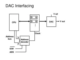
Interfacing • CPU vs. I/O Bound • Buffered vs. Unbuffered • Synchronization • Blind cycle • Busy polling • Interrupts • vectored • Direct Memory Access (DMA) • I/O Modules/Ports • isolated • memory mapped
CMOS I/O structures see Wakerly 3.3 - 3.7, pp 86 - 135 • Schmitt Trigger Inputs • Tri-State Outputs • Hi-Z(impedance) state: effectively disconnection from circuit. • Open Drain Outputs • floating output requires pull up resistor(small) connection to positive voltage.
I/O Port Pin shared: Tri-State Output D- Latch Input • Two control registers TRISx and PORTx • bsf/bcf use a read/write back cycle • Be careful when changing TRISx mid-operation
Timing/Delay delay_1ms movlw 0xF9 ; 0xF9 = 249 nop usec4 addlw 0xFF ; add -1 btfss STATUS,Z goto usec4 return • Count the instructions (know the clock frequency) • Use the timers • Watchdog • nominal time-out period of 18 ms. Period varies with temperature,VDD • Scale up to 1:128 (max. 2.3 seconds) • reset/wake-up on timeout • Timer0/1/2 • period determined by external oscillators or the instruction cycle • pre/post scaling • poll for timeout/interrupt on timeout
Polling Init bsf STATUS,RP0 ; bank 1 movlw B'00100110' ; set in counter mode, prescaler = 128 movwf OPTION_REG bcf STATUS,RP0 ; back to bank 0 bcf INTCON,T0IF ; clear to be sure . . call Delay . . Delay movlw 106 ; time for 256 - 106 = 250 cycles movwf TMR0 bsf STATUS,RP0 ; switch to bank 1 to access OPTION_REG bcf OPTION_REG,T0CS ; start timing bcf STATUS,RP0 Loop btfss INTCON,T0IF ; keep checking for overflow goto Loop bcf INTCON,T0IF ; clear flag return
Interrupts • Global Interrupt Enable Bit • Individual interrupts • Interrupt Enable Bit • Interrupt Flag Bit • Registers • INTCON, • PIR1, PIR2, PIE1, PIE2
Interrupt sample code ISR movwf w_temp ; save W and STATUS movf STATUS,W ; movwf status_temp ; Poll btfsc INTCON,TOIF ; test if TMR0 overflow occurred call Timer_hndlr ; call handler for TMR0 btfsc INTCON,INTF ; test if external interrupt occurred call Extern_hndlr ; call handler for external interrupt btfsc INTCON,RBIF ; test if PORTB change interrupt occurred call Change_hndlr ; ...etc movf status_temp,W ; restore pre-isr STATUS register movwf STATUS ; swapf w_temp,F ; restore pre-isr W register contents swapf w_temp,W ; ... without affecting the zero flag retfie ; return from interrupt Timer_hndler bcf INTCON,TOIF ; clear the overflow flag ; do processing return Extern_hndlr ; clear appropriate flag etc return Change_hndlr ; clear appropriate flag etc return
Simple I/O • LEDs • source/sink (check current!) • 7 segment displays • common anode (sink) • common cathode (source) • multiple digits: cycle • Switches • software debounce • hardware debounce (Schmitt Trigger) • Shared pin for I/O • DO NOT enable the external I/O device inputs when reading the external outputs.
External Parallel Bus • Bus lines • selection/address lines • data lines • read, write lines • Master • PIC controls access to I/O devices/modules • any I/O port may be used • PIC must adhere to timing • Slave • Another microprocessor accesses data on the PIC • PSP port must be used. • Master must adhere to timing • Interrupt on read/write
Hitachi 44780 LCD • Synchronous Parallel bus • read/write line; data lines • instruction/register select • clock/enable • Alternative: Serial interface chips • specific to 44780 • general serial to parallel converters
PSP • Operation performed in Q2 • Flags set at start Q4 (except OBF which follows RD) • External Master holds signals for 5*Q
A/D conversion techniques • Parallel encoding • Compare the input voltage to a series of equally spaced reference voltages • Each comparator outputs a single bit of the digital value • FAST (all bit simultaneous) but large circuit • Successive approximation • Use a DAC, and binary search until the DAC output matches the input voltage. • Digital value is the final DAC input • Time proportional to number of bits • Dual slope integration • Allow capacitor to charge for a fixed time • Digitally time the discharge for a constant current output • Discharge time is proportional to input voltage See “Art of Electronics” Horowitz pp.622-624
From: http://niuhep.physics.niu.edu/~labelec/lect/p475_lect242.pdf
Joystick port • 8 bit I/0 card • ISA bus I/O address 201h • Write: starts position measurement. • Read: The bits are mapped in the value you get, as:_______________________________________________________ | 7 | 6 | 5 | 4 | 3 | 2 | 1 | 0 | | but4 | but3 | but2 | but1 | stk4 | stk3 | stk2 | stk1 | |______|______|______|______|______|______|______|______| • Buttons: 0=closed, 1=open (default) • Monostables: 1=timing, 0=timed-out (default) http://www.epanorama.net/documents/joystick/pc_joystick.html
From: http://niuhep.physics.niu.edu/~labelec/lect/p475_lect242.pdf
PIC 16F877 A/D Block diagram 8 channels; 10 bit resolution; left/right justification; reference voltage configuration ADCON1
Sampling Time=Acquisition Time+ Conversion Time • For correct A/D conversions, the A/D conversion clock (TAD) must be selected to ensure a minimum TAD time of 1.6 ms. • Between A/D conversions or after switching channels, the minimum sampling time must be observed (to avoid bad readings).
D/A conversion techniques • Scaled resistors • connect all bits via different resistor values to an op-amp • each resistor should be twice the value of the resistor for the next most significant bit. • R-2R ladder • instead of inputting scaled 0/1 voltages, voltage inputs are switched from a “ladder” made up of 2 resistor values • Pulse Width Modulation • a train of pulses is generated, whose on-width per period is determined by the digital value • the average voltage value of the pulse train is proportional to the digital value. • A low pass filter (RC) can be used to produce an averaged signal. See “Art of Electronics” Horowitz pp.612-621
PWM Theory • Duty Cycle often expressed as a percentage of the period. • Average output voltage will be approximately the same percentage of the “on” voltage. • Typical uses: • ideal for loads with slow response (no capacitive filtering necessary) • Intensity control • Motor control • Temperature control
PWM in PIC16F877 • Software: Timer interrupt • Hardware: PWM module • Calculate of period and duty cycle times: • instruction frequency 1MHz (4MHz clock) • instruction cycle time TCY=1s • pre-scale ratio 1:8 (LAB2 formula) • For scale: 1:64; timer overflow cycle time 64 s • Desired frequency 60Hz, 16.6ms, 260 ticks • Duty Cycle: Period (ticks) by %on-time • For an A/D reading 0-255 we can presume that the duty cycle is equal to the reading for a 60Hz PWM. • Points to note: • minimum/maximum frequencies:eye/ear • frequency granularity: # steps • signal noise -- the CCP/PWM outputs are near to oscillator input lines! • current switching: isolate through transistor.
PIC16F877 PWM Example • 16 MHz oscillator • Required PWM: • Period -- 1ms • On-time resolution -- 1s • Two possible solutions: • use one of the two CCPx pins with the built in PWM function and Timer2. • use any generic port pin Rxn with software interrupts from Timer0, 1 or 2
963/4 = 240.75 11110000 CCPR1L 11 CCPCON<5:4> Built-In PWM • Find the instruction cycle time: • FOSC =16MHhz • FCYC =16/4=4MHz • TCYC =0.25s • Period 1ms = 1ms/0.25 s = 4000 instruction cycles • Choose TMR2 (8 bit) pre-scale: • 1:1 -- max. 256 instruction cycles • 1:4 -- max. 1024 instruction cycles • 1:16 -- max. 4096 instruction cycles • PR2 Value = 4000/16 -1=249 • Resolution • TMR2 will count in increments of 16*0.25 s = 4 s • CCPR1L Value = OnTime (s)/4 • To get 1 s resolution we need all ten bits e.g. 963 s
Software -- PWM by force • Find the instruction cycle time: • FOSC =16MHhz • FCYC =16/4=4MHz • TCYC =0.25s • Period 1ms = 1ms/0.25 s = 4000 instruction cycles • Choose which timer and what pre-scale value: • Timer0: 8 bits; pre-scaler 1:1/2/4/8/16/32/64/128/256 • Timer1: 16 bits; pre-scaler 1:1/2/4/8 • Timer2: 8 bits; pre-scaler 1:1/4/16 • Timers 0,2 will give a 4 s increment; to get 1 s resolution we will need to implement a software fraction • Timer 1 can give use a 0.25 s increment; with a pre-scaler of 4 this will automatically be a 1 s increment.
ORG 0x04 goto ISR ISR movwf _w movf STATUS,w movwf _status btfsc PWM goto PWM_ON PWMOff nop bsf PWM movf Ontime,W goto PWM_Done PWMOn bcf PWM movf Ontime,W subwf Period,W nop PWMDone sublw 0 movf TMR0 bcf INTCON,T0IF movf _status,W movwf STATUS swapf _w,F swapf _w,W retfie 1,2 3 4 5 6 7,8 9 10 11 12 ,7 8 9 10 11,12 13 14 15 16 17 18 19 20,21 Sample ISR -- 21 Cycles
Sample ISR--21 cyclesPoints to Note • Variable PWM predefined #define PWM PORTx,n • no interrupt flag polling, presumes that TMR0 is the only interrupt • nop s are used to keep the branches aligned • PWM is set and clear at instruction 9 in both branches • Both branches hit PWM_Done at instruction 13 • Two’s complement the desired time, to get the starting value for TMR0 sublw 0
TMR0 - 1:16 prescaler Period = (1ms/0.25s - 2*Interrupt Run time)/16 OnTime = (pulse width/0.25s - Interrupt Run time)/16 Ideal Interrupt Run Time is a multiple of 16. Modify the routine using additional nop to meet the requirements. Resolution is limited only by the clock period 0.25 s. Define Fraction as the number of additional instruction cycles required -- it will be used to delay the onset of the OFF time in the ISR. Fraction = (pulse width/0.25 s)/16 *16 - (pulse width/0.25 s) Fraction OnTime TimerIncrement Period
PWMOn movf Fraction,W sublw 0 addwf PCL, F nop nop nop nop nop nop nop nop nop nop nop nop nop nop nop bcf PWM movf Fraction,W addwf PCL, F nop nop nop nop nop nop nop nop nop nop nop nop nop nop nop movf OnTime,W subwf Period,W PWMOff nop nop nop nop bsf PWM nop nop nop nop nop nop nop nop nop nop nop nop nop nop nop nop movf OnTime,W goto PWMDone 1 2 3 4 5 6 7 8 9 10 11 12 13 14 15 16 17 18 19 20 21 22,23 1 2 3 4 5 6 7 8 9 10 11 12 13 14 15 16 17 18 19 20 21 22 23 ISR call cycles 2 Pre-branch cycles 8 Branch cycles 23 Post-branch cycles 9 42 Nearest 16 multiple 48 nops required before retfie 6 A possible revised ISR
A possible revised ISRPoints to note • Fraction resolution of 0.25 s exceeds specification of 1 s • OnTime has a lower limit of 48/16=3 Timer0 increments =12 s • Period=(4000-2*48)/16=244 • The revised ISR will occupy significantly more code-space, due to the use of all these nop s
Serial Communication • Error Detection Overhead • Single Dataword • Parity: Even, Odd, Mark, Space,None • Start/Stop bits • Packet/Frame • ByteCount, Checksum, CRC • Packet ID, Acknowledge • SOF/EOF; Header/Trailer • Single / Multi-user • Dedicated • (optional) Handshaking/Signalling • Network • Receiver/Sender ID • Arbitration/Collision detection
Serial Communication Protocols • Synchronous • Microwire • SPI • I2C • Asynchronous • RS232 • RS485/422 • Manchester • CAN • Dallas Semiconductor 1-wire interface • All can be implemented with I/O Ports. • PIC16F877 has built in support for some. • MSSP • USART
MPLAB-SIMInstruction Level Simulator Limitations • No A/D result loaded • PWM resolution > instruction cycle • Additional clock pulse inputs > instruction cycle • No support for serial I/O simulation: one alternative is pin stimulus and stopwatch. • No compares > 8 bits (CCP)