Hybrid Pixels Development for High-Energy Physics Research
Discover the innovative hybrid silicon pixel detectors enabling cutting-edge research in high-energy physics. Learn about the development milestones, technologies, advantages, and latest advancements in the field.

Hybrid Pixels Development for High-Energy Physics Research
E N D
Presentation Transcript
BTeV Hybrid Pixels David Christian Fermilab July 10, 2006
Context • BTeV was possible because of two “enabling technologies.” • A silicon pixel detector with very high segmentation and very fast, zero suppressed, readout. • A vertex trigger (using pixel hits) capable of accepting data from more than 15 million events per second, selecting events containing measurable b decays, and rejecting backgrounds.
Advantages of hybrid silicon pixel detectors • Excellent spatial resolution • High stopping power of silicon: • Most ionization is contained within a few microns of a track. • A minimum ionizing particle creates 80 e/h pairs per micron of track length. • Low noise electronics: • Small sensor pixel and bump bonding means very small input capacitance. • Separate development of sensor and readout chip allows each to be optimized.
Status as of February 2005 • Sensor module R&D complete • Licensed use of “moderated p-spray” n-in-n technology developed for ATLAS • Chip development near completion • Two failures must be corrected: • Readout hangs when multiple pixels are hit in ~200ps interval as BCO number is incrementing (design change is done). • Amplifier oscillates after irradiation with large leakage current. • Other readout/mechanical design well advanced (but BTeV-specific).
The last 16 months • Proposal to finish development of BTeV pixels in the context of ILC detector R&D was approved in May, 2005. • Construction of a pixel telescope for the forward arm of PHENIX is a part of this. • Final readout chip (FPIX2.1) has been tested. • Both faults have been corrected. • A “general purpose” HDI has been designed and fabricated.
FPIX2 at a glance • Designed to be the BTeV pixel chip. • 50m x 400m pixels (like ATLAS). • 22 columns x 128 rows. • Designed to tile chips in one line with 600m long pixels between chips; not designed to tile two lines of chip on one sensor module. • High speed, zero suppressed readout. • Can be ~30ns/hit. • All chips read out in parallel on point-to-point links. • NO TRIGGER. • Easy to use. • One bias voltage (+2.5V) • All LVDS I/O – No other ASIC’s required.
FPIX2 Block Diagram Pixel Unit Cells (22 columns of 128 rows each) Core Fabricated by TSMC (through MOSIS). Only bias voltages required are 2.5V & ground. All I/O is LVDS. End-of-Column logic (22 copies) Core Logic DAC’s Clock Control Logic Next Word Block Data Output Interface Programmable Registers Word Serializer Programming Interface Steering Logic Data Output Clock BCO Clock Input/Output High Speed Output
- + 00 - idle 01 - reset 10 - output 11 - listen Pixel Unit Cell Vdda Thresholds (Vth1-Vth7) Token Out ADC Thermometer Flash Latch to Binary Vfb2 Encoder Resets Row Address Bus Command Interpreter Controller Sensor Kill Inject Test Vref Threshold (Vth0) 4 pairs of RFastOR Throttle Read Clock HFastOR Command Lines Read Reset Token In Token Reset
Pixel Cells (four 50 x 400 mm cells) 12 µm bump pads Preamp 2nd stage +disc Kill/ inject ADC encoder Digital interface ADC (Top metal layer not shown)
Bump bonds Wire bonds Silicon Sensor 250 µm 50 µm 200 µm 210 µm FPIX2 HDI Pixel Module NOT TO SCALE
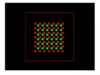
Detector building blocks • Pixel size = 50 microns x 400 microns • Readout chip services 22 columns of 128 rows of pixels • Module = Single row of readout chips bonded to a sensor (4,5,6, or 8 readout chips) • Active area of 8x module = 73.6mm x 6.4mm; current HDI is 104.5mm x 11.1mm.
A possible building block 36.8 mm