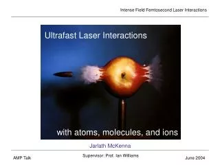

Ultrafast sensors For the Future
E N D
Presentation Transcript
A/Prof. C. Tripon-Canseliet UPMC - Université Pierre et Marie Curie – Electronics and Electromagnetism Lab (L2E) - France In cooperation with THALES Airborne Systems - France IEMN- Electronics , Micro and Nanotechnologies Institute – France Nanyang Technological University/CINTRA – Singapore Ultrafast sensors For the Future
Optics metrology for electronics: specific needs for industrial applications Electronics technological bottleneck: high frequency activation and functionality Electronics/Electronics: DC to microwave domain Optics/Optics: Terahertz domain Optics/Electronics: Microwave to sub-mm range Optics for classical electronic clock jitter limitations overcoming Optical laser sources: highest resolution for electronic systems Semiconductor technological procees: Integration access Optics for ultra short pulse bandwith generation Femtosecond risetime Speed of light Few tens to hundred fs time bandwidth: Highest external control frequency Demonstration of optics in RF electronic systems: Active research field Ligth/matter interactions Integration of optics for microwave fucntionalities Nanotechnologies for improvment Researchstrategy RF carrier generation RF magnitude switching RF phase shifting RF amplification Introduction PC effect Introduction
Identified efficient RF functunalities for industrial applications: State-of-the-Art in microwave photonics All optical signal processing Beam scanning of antennas arrays (True Time Delays) Very low noise generation (by signal injection) Radio over Fiber (RoF) systems (high data rates > 100 Gbits/s) Technological support for systems integration Building blocks Sources (Lasers, LEDs) Receivers (Photodiodes, photo transistors) RF information transport on optical carriers (AM/PM/FM) Information support (Optical waveguides) Physical limitations scanning: Why not Nanoscale? Confinement of light/matter interactions with diffraction effects Nanotechnology platform access Researchstrategy RF carrier generation RF magnitude switching RF phase shifting RF amplification Introduction PC effect Introduction Free space Guided space Micro integration Nano integration ?
One example among others: High frequency sampling George Valley chart « Three Ten law »: 10 GHz – 10 fs – 10 Bits Researchstrategy RF carrier generation RF magnitude switching RF phase shifting RF amplification Introduction PC effect Introduction Sampling pulses Opening time Time Jitter Optical clock need DV Opening uncertainty
Ligth/Matter interactions inventory: How we can play with light…. Light emission (Photoluminescence, Electroluminescence) Light Absorption Light scattering Rayleigh scattering Brillouin scattering Raman scattering Optical rotation Case of bulk materials Researchstrategy RF carrier generation RF magnitude switching RF phase shifting RF amplification Introduction PC effect Introduction Critical parameters Anisotropy of media Polarisation state of light
Photoconductive effect description Photoconductivity of semiconconductor materials (GaAs, GaAs BT) Generation of electron/hole pairs: Material conductivity enhancement Local photoresistance Semiconducting materials family Energy band gap Absorption coeffcient( ~104 cm-1) Carriers dynamics Resistivity Optical command Time domain shape Source compactness waveguide Researchstrategy RF carrier generation RF magnitude switching RF phase shifting RF amplification Introduction PC effect Introduction
Nano material-based microwave devices under optical control for next generation of EM sensors Material and components approach : Physics, design, simulation, modeling New semiconductors Carbon nanotubes Semiconductor Nanowires Metal/dielectric or Metal/semiconductor interfaces Devices and functions approach Physics, design, simulation, modeling Modulation by SPP generation Nano RF magnitude switching Nano RF beam scanning by nano antennas (RF au THz) Introduction RF carrier generation RF magnitude switching RF phase shifting RF amplification Researchstrategy PC effect Research strategy Characterization Characterization Associated signal processingfunctions
Microwave photonic characterization platform (UPMC) Frequency and transient measurements (DC – 67 GHz) CW laser sources (0.8 – 1.3 and 1.55 µm) Femtosecond fibered and tunable laser source (0.8 and 1.55 µm) Probe test environnement setup under specific thermal conditions Electrical and electromagnetic multiscale and multiphysic Design platform (UPMC) Photoconductive effect homemade transient modeling in ADS software Carriers time varying density equivalent electrical modeling Associated time varying photoresistance Optical command characteristics power, spot size, wavelength Carriers dynamics (mobilities and lifetimes) Semiconducting material dark resistivity Microwave circuit transient and frequency (after FFT) behaviour in microwave domain Photoconductive effect design tool in 3D electromagnetic software Introduction RF carrier generation RF magnitude switching RF phase shifting RF amplification Researchstrategy PC effect Research strategy
Actions plan (2008 – 2013) Introduction RF carrier generation RF magnitude switching RF phase shifting RF amplification Researchstrategy PC effect Research strategy Nano RF engineering Architecture Design Classical RF engineering Architecture Design Nano RF engineering Architecture Design Bulkmaterials GaAs, GaAs BT (0.8 µm) GaAs Sb (1 µm) GaAsSbN (1.55 µm) Nano materials implementation Nanowires (GaAs) SW and MW Nanotubes (C) Nano materials study Nanowires (GaAs) SW and MW Nanotubes (C) Surface effects (SPP) Thrust 1 Thrust 3 Thrust 2 Carriers dynamics (Mobiliies, lifetimes) Dark resisitivity Carriers transport (balisitc regime) Integration with MMIC planar technology (Process or deposition methods eligibility) Nano electromagnetism under infinite boundaries (Limitations of classical electromagnetics) Feasibilty of transmission of RF signals in nano access Interconnections Limitations under finite boundaries Arrays functionalities – Densification Nanoscale coupling effects
Photoconductive effect homemade modelling (1/2) Microwave signal processing by optics Carrier density evolution in time under time-varying optical illumination Introduction RF carrier generation RF magnitude switching RF phase shifting RF amplification Researchstrategy PC effect Photoconductive effect Substrate permittivity loss angle height carriers mobility +carriers lifetime + doping Output parameters Input parameters Time domain photoresistance Rg(t) Optical signal transient shape (magnitude, frequency modulation) Microwave switch dimensions (integrated technology) S-parameters (Fourier transform) Substrate parameters
Photoconductive effect homemade modelling (2/2) Non linear electical modelling: Real-time control of microwave signals by optics Introduction Researchstrategy RF carrier generation RF magnitude switching RF phase shifting RF amplification PC effect Photoconductive effect fmod= 1 GHz Carriers densities (/cm3) RF output signal RF input signal Time (ns) Demonstration of modulation signal carrier transfert from optics to microwave carrier fRF = 10 GHz - fmod= 1 GHz Δτ = 50 ps Time (ns)
Photoconductive effect in microwave circuit: classical behaviour in microwave domain Integration in a microwave circuit with line discontinuity Magnitude switching / Phase shifting (high pass filter behaviour) Microwave functionalities demonstration Modulation transfer Ultrafast sampling Digital coding with high data rate and Bits resolution access Ultrafast clock trigerring thanks to very low jitter optical source Generation Integration in MMIC ascillator on standard GaAs substrate Introduction Researchstrategy RF carrier generation RF magnitude switching RF phase shifting RF amplification PC effect Photoconductive effect Side view of microwave photoconductive switch Associated RF efficiency
Photoconductive effect for 5 GHz carrier generation Integration in MMIC ascillator on standard GaAs substrate Introduction Researchstrategy RF magnitude switching RF phase shifting RF amplification RF carrier generation PC effect Microwave carrier generation by optics Oscillator tuned spectrums obtained by triangular modulation of incident optical power (fmod 50 KHz,λ = 800 nm,) (1) 0–80 mW, (2) 0–130 mW and (3) 0–180 mW Measured transient Optically generated microwave carrier at a frequency of 5GHz MMIC top view (UMS PH25 foundry process) S. Faci, C. Tripon-Canseliet, G. Alquié, S. Formont, , J. Chazelas “Ook modulator using photoconductive feedback oscillator” Microwave and opticalTechnologyLetters, Vol 52, Issue 9, pp.2010-2016, Sept 2010 S. Faci, C. Tripon-Canseliet, A. Benlarbi-Delaï, G. Alquié, S. Formont, , J. Chazelas “Optical generation of microwave signal for FMCW radar applications”, Microwave and opticalTechnologyLetters, Vol 51, Issue3, pp.690-693, March 2009
Photoconductive effect for 5 GHz carrier generation Ultrafast pulse illumination: Real-time control of microwave carrier generation by optics RF transient output (200 ps/div) Introduction Researchstrategy RF magnitude switching RF phase shifting RF amplification RF carrier generation PC effect Microwave carrier generation by optics Experimental results @ 5 GHz MMIC top view (UMS PH25 foundry process) Optional tunability by DC bias RF signal setting time (50 ps) RF signal time window Optional tunability by optics RF signal frequency RF signal time window period RF transient output (1ns/div) S. Faci, C. Tripon-Canseliet, G. Alquié, S. Formont, , J. Chazelas “Ook modulator using photoconductive feedback oscillator” Microwave and opticalTechnologyLetters, Vol 52, Issue 9, pp.2010-2016, Sept 2010 S. Faci, C. Tripon-Canseliet, A. Benlarbi-Delaï, G. Alquié, S. Formont, , J. Chazelas “Optical generation of microwave signal for FMCW radar applications”, Microwave and opticalTechnologyLetters, Vol 51, Issue3, pp.690-693, March 2009
Photoconductive effect for ULB signal generation and emission Integration in a microwave circuit: Microwave functionalities demonstration UWB signal generation by ultrafast optical control with optically-controlled signal waveform shaping Introduction Researchstrategy RF magnitude switching RF phase shifting RF amplification RF carrier generation PC effect Microwave carrier generation by optics Experimental setup for optically-controlled UWB emitting system Experimental UWB photogenerated signal Transfer function of the system Transient response of the emission antenna Simulated and measured reflection coefficient of the UWB antenna Guldner, N.; Tripon-Canseliet, Faci, S., C.; Alquie, G. “Optically-controlled UWB emission system” IEEE MicrowaveConference, 2009 (EuMC), 2009, Page(s): 1916 - 1919
ON/OFF ratio enhancement under CW illumination: Confinement intensification Membrane material RF circuit mismatching (at OFF state) Introduction Researchstrategy RF carrier generation RF phase shifting RF amplification RF magnitude switching PC effect Microwave magnitude switching by optics • Carriers densityincrease • Capacitive behaviourlowering • Optimization of RF access design Interaction volume: 20x20x2 µm3 Interaction volume: 1x1x0.5 µm3 C. Tripon-Canseliet, S. Faci, K. Blary, G. Alquié, S. Formont, J. Chazelas SPIE International Conference on Application of photonicTechnology, Quebec, Canada, June 2006 DGA contract n° 07.34.014 (2007-2010) Partners: IEMN and THALES Airborne Systems
ON/OFF ratio enhancement under CW illumination: Confinement intensification Nanotechnology-based MPCS @ 0.8 µm Dielectric nano waveguide implementation Introduction Researchstrategy RF carrier generation RF phase shifting RF amplification RF magnitude switching PC effect Microwave magnitude switching by optics • Si, SiGe, GaAsnanowiresimplementation 0.5 µm Experimental values of a SI GaAs photoconductivity under 0.8µm optical illumination 2009 MERLION program (French Embassy @ Singapore)– Nw-basedelectronics Partnership: IEMN- UPMC- NTU
Nanotechnology-based MPCS @ 1.55µm: Quaternary semiconducting material buk material Study of photoconductivity of quaternary semiconductors (GaAsSbN) Design and tests of optically-controlled microwave switches Introduction Researchstrategy RF carrier generation RF phase shifting RF amplification RF magnitude switching PC effect Microwave magnitude switching by optics Carrier lifetime measurement @ 1.2 -1.55 µm MPCS substrate structure Experimental magnitude ON/OFF ratio @ 1.55 µm in frequency 2008 MERLION program (French Embassy) grant GaAsSbNprocess for optoelectronics Partnership: IEMN-UPMC- NTU • ANR/ A star joined program grant • noveldilutenitride III-V Compound sEmiconductoR for 1550nm Ultra-FastPhotoconductIveSwitchE (CERISE) • Partnership: IEMN-UPMC – THALES - NTU K.H. Tan, C. Tripon-Canseliet, S. Faci, A.Pagies, M. Zegaoui, W. K.Loke, S. Wicaksono, S. F. Yoon, V. Magnin, D. Decoster, and J. Chazelas, IEEE PHOTONICS TECHNOLOGY LETTERS, VOL. 22, NO. 15, AUGUST 1, 2010 K. H. Tan, S. F. Yoon, C. Tripon-Canseliet, W. K. Loke, S. Wicaksono, S. Faci, N. Saadsaoud, J. F. Lampin, D. Decoster, and J. Chazelas, APPLIED PHYSICS LETTERS 93, 063509 2008
Nanotechnology-based MPCS @ 1.55µm: CNT-based technology Modeling and characterization of RF behaviour of MW or metallic SW CNTs Study of photoconductivity of semiconducting SW CNTs under polarized Design and test of CNT-based RF nano emitters Design and tests of optically-controlled microwave phase shifters Introduction Researchstrategy RF carrier generation RF magnitude switching RF amplification RF phase shifting PC effect Microwave phase shifting by optics CNT A. Maiti, Caron Nanotubes: Band gap engineering with strain, Nature Materials 2 (2003) 440 J. Guo, M. A. Alam, Y. Yoon, Appl. Phys. Lett. 88, 133111 (2006). SEM photograph of vertical MW CNT processed by PECVD @ NTU • DGA/DSTA joinedprogram grant • Nano antennas • Partnership: IEMN-UPMC – THALES - NTU Examples of RF reflective (a) and filtering (b) structures for CNT RF properties extraction
Research work focus (since 2007): Nanotechnology-based emitting system @ 1.55µm Study of photoconductice of SW CNT-based FET with transparent electrodes (ITO) Design and tests of optically-controlled microwave amplifier with reported matching circuit in hybrid technology Introduction Researchstrategy RF carrier generation RF magnitude switching RF phase shifting RF amplification PC effect Microwave amplification by optics Laser excitation Nano RF amplifier Active quadripole • ANR program grant • MicrowaveOptically-ControlledCnt-basedemitting Architecture • Partnership: IEMN-UPMC – THALES - NTU
Eligibility by experimental demonstration of nano material efficiency in dynamic regime Nano wires/tubesl arrays Nano ribbons/cristals/shells Extension of existing modeling and design tools to mutliscale components and devices Prospect new technological process/deposition methods to open access to low cost components fabrication Optimization of existing nano materials integration for microwave photonic purposes Electronic access Light interaction effects (plasmonics) Introduction Researchstrategy RF carrier generation RF magnitude switching RF phase shifting RF amplification PC effect Prospects M. S. Islam, N. P. Kobayashi, S-Y. Huang 2008 2nd IEEE International NanoelectronicsConference (INEC 2008), p.1009-1014
Acknowledgments • Collaborators • G. Alquié (L2E) • D. Decoster (IEMN) - Professor • J. Chazelas (THALES) – TechnicalDirector • K.L. Pey (NTU previously - now @SUTD) - Professor • Yoon S.F. - Tay B. K (NTU/EEE school) - Professors • D. Baillargeat (CINTRA) - Professor • PhDstudents and Post Docs • S. Faci – K. Louertani - N. Guldner – B. Guillot (L2E) • N. Saassaoud / M. Zegaoui / A. Pagies/ (IEMN) • A. Olivier (CINTRA/IEMN) • Teo E. – Tan D. Mimicking the Human being Nanotechnologies Thank you for your attention Charlotte.tripon-canseliet@upmc.fr
Trust 1 : Study of metallic/semiconducting interfaces DGA contract n°08.108.38 - Partners: IEMN – Thales Research and Technology Solution for confinement of light for RF modulation of optical carriers Design, fabrication and characterization of a fully-integrated device nd R nd + Δn ΔR z θi kr θ n1 θr Ei Er ki Δn(V) = nd cos(wmt) x kx θt n2 kt Incident beam Incident beam Et Prism Prism Attenuated beam Metal Dielectric Surface plasmon Dielectric Metal Otto configuration Kretschmann configuration Research actions plan
Nanotechnologies: performances attendues Propriétés électriques Résistivité/conductivité, résistance de contact avec différents métaux Propriétés électroniques Transport / Dynamique des électrons (mobilités, vitesse de transit, temps de vie) Propriétés optiques Structure de bande / Sensibilité en longueur d’onde (Bande spectrale d’absorption) Propriétés thermiques Propriétés mécaniques Techniques de fabrication Nano objets: vers des propriétés surprenantes Propriétés des CNTs compoarées aux matériaux semiconducteurs connus Résisitivté de nanofils d’InN – Résistivité avec et sans résistance de contact (Méthode à 4 pointes en noir) P. Avouris, M. Radosavljevic, S. J. Wind, CNT electronics and optoelectronics, NanoScience and Technology, Applied Physics of Carbon Nanotubes, Fundamentals of Theory, ISBN 978-3-540-23110-3 F. Werner, F. Limbach, M. Carsten, C. Denker, J.Malindretos, A. Rizzi, Nano Lett., Vol. 9, No. 4, 2009
Nanofils: Méthodes de fabrication pour composants électroniques et optoélectroniques Structures homogènes Jonctions PN Transistors FET MOSFET Nano engineering Approche « Bottom-up »: croissance catalysée Approche « Top-down »: gravure verticale Mise en réseau de nanobjets Nano objets: Propriétés optoélectroniques Y. Li, F. Qian, J. Xiang, and C. M. Lieber MaterialsToday, Oct. 2006, 9, 10
Exemple de nanofils d’InP Caractérisation optique: Electroluminescence Nano objets: Propriétés optoélectroniques X. Duan, Y. Huang*², Y.Cui, J.Wang* & C.M. Lieber, Nature, 409, Jan 2001, p.66-68 p-n junction 5 µm Diam: 65 et 68 nm 5 µm Diam: 39 et 49 nm
Exemple de nanofils de Si Caractérisation optique : photoluminescence Nano objets: Propriétés optoélectroniques M.-H. Kim , T.-E. Park, U.-K. Kim, H.-J. Choi, G.-Y. Sung, J.- H. Shin, K. Suh 2007 4th IEEE International Conference on group IV Photonics, Page(s): 1 - 3 Th Stelzner, M Pietsch, G Andra, F Falk, E Ose and S Christiansen Nanotechnology 19 (2008) 295203
Nanofils hétérostructurés (GaAs/GaP) Caractérisation statique I(V) et optique (électroluminescence) Nano objets: Propriétés optoélectroniques Gudiksen, M., et al., Nature (2002) 415, 617 Wu, Y., et al., Nature (2004) 430, 61
Nanofils hétérostructurés (GaN/InGaN/GaN/AlGaN/GaN) Caractérisation statique I(V) et optique (électroluminescence) Nano objets: Propriétés optoélectroniques Qian, F., et al., Nano Lett. (2005) 5, 2287
Nanotubes de Carbone Propriétés optoélectroniques Jonctions PN: Electroluminescence Nano objets: Propriétés optoélectroniques Chen, J., et al., Science (2005) 310, 1171
Nanotubes de Carbone Représentation par un enroulement d’une feuille de graphène (arrangement 2D d’atomes de Carbone) Nature métallique ou semiconductrice déterminée par Diamètre Type d’enroulement (mono/multi paroi) Chiralité Propriétés électroniques Mobilités Résistivité Nano objets: Propriétés optoélectroniques
Nanotubes de Carbone Propriétés optoélectroniques Photoconductivité: Dépendance en polarisation Nano objets: Propriétés optoélectroniques J. Guo, M. A. Alam, Y. Yoon, Appl. Phys. Lett. 88, 133111 (2006). X. Qiu, M. Freitag, V. Perebeinos, P. Avouris Nano Lett. 5, 749 (2005).
Nano objets: Propriétés optoélectroniques • Nano objets : Synthèse • Composants électroniques: Diodes, Transistors Applications industrielles: circuits logiques (Mémoires) • Composants optoélectroniques: LEDs, (Photodiodes PIN) Applications industrielles: Ecrans Composants pour applications RF Utilisation des propriétés optiques Nano dispositifs intégrés à contrôle optique
Commande optique CW: Commutation d’amplitude Recherche du confinement de l’interaction Augmentation de la densité de porteurs Diminution du comportement capacitif RF du dispositif Premiers travaux effectués au L2E (2006) Structure membrane Augmentation de l’impédance des lignes d’accès: Réduction de la zone d’interaction Dispositifs intégrés RF à contrôle optique C. Tripon-Canseliet, S. Faci, K. Blary, G. Alquié, S. Formont, J. Chazelas SPIE International Conference on Application of photonic Technology, Quebec, Canada, Juin 2006
Commande optique CW: Commutation d’amplitude Recherche du confinement de l’interaction lumière/matière pour la commutation d’amplitude par l’optique Réduction de la zone d’éclairement Dispositifs intégrés RF à contrôle optique
Exemple de nanofils d’InP Caractérisations statiques I(V) Application à des jonctions croisées Nano objets: Propriétés optoélectroniques 10 nm Ni/In/Au contact electrodes 10 mm Diam: 29 nm Diam: 40 nm p-p Diam: 47 nm 2 mm 1 mm Ni/In/Au contacts n-n n-p Diam: 45 nm 1 mm X. Duan, Y. Huang, Y.Cui, J.Wang & C.M. Lieber, Nature, 409, Jan 2001, p.66-68
Exemple de nanofils de Si Caractérisation statique de transistors à effet de champ Nano objets: Propriétés optoélectroniques 500 nm 100 nm channel length Vds@-0.8V Vds@-10 mV J. Martinez, R.V. Martinez, R. Garcia, IEEE-NANO 2009. 9th IEEE Conference on Nanotechnologies, Page(s): 442 - 443 H. Lu et Al, Nano Letters(2008), 8, 925
Exemple de nanofils de Si (méthode top-down améliorée) Caractérisation statique I(V) Nano objets: Propriétés optoélectroniques Jing Zhuge; Yu Tian; Runsheng Wang; Ru Huang; Yiqun Wang; Baoqin Chen; Jia Liu; Xing Zhang; Yangyuan Wang; IEEE Transactions on Nanotechnology,9 , Issue 1, 2010, Page(s): 114 - 122
Hybridation et mise en réseau de Nanofils (méthode Bottom-up) Caractérisation statique I(V) Nano objets: Propriétés optoélectroniques M. S. Islam, N. P. Kobayashi, S-Y. Huang 2008 2nd IEEE International Nanoelectronics Conference (INEC 2008), p.1009-1014