Download

1 / 9
90 likes | 291 Vues
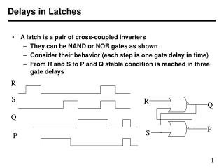
R. Q. P. S. Delays in Latches. A latch is a pair of cross-coupled inverters They can be NAND or NOR gates as shown Consider their behavior (each step is one gate delay in time) From R and S to P and Q stable condition is reached in three gate delays. R. S. Q. P. D. D. Q. Q. D. P.

E N D
R Q P S Delays in Latches • A latch is a pair of cross-coupled inverters • They can be NAND or NOR gates as shown • Consider their behavior (each step is one gate delay in time) • From R and S to P and Q stable condition is reached in three gate delays R S Q P
D D Q Q D P P G G C R R R Q Q Q D Q D P P P D D D S S S G P G G G C Delays in Gated-Latch and Flip-Flops • G acts as a control signal in a gated latch • G = 0 means no writing, G = 1 allows writing • In an edge-triggered flip-flop, data is written in flip-flop upon arrival of a clock edge • This is achieved by connecting two gated latches as shown • Actual implementation may be slightly different, concept is same
R R Q Q D P P D D S S G G C Timing Issues in D Flip-flops • When C is low, second gated latch does not record anything, but the first latch samples the D-input • Before the clock changes from low to high • Changes in D propagate through many gates to output. Therefore D should be stable for at least five gate delays • This represents the set up time of a flip flop • When clock changes from low to high • The first latch may still sample up to two gate delay time. Therefore, D should remain stable even after clock changes • This is called the hold time of a flip flop
O U T P U T S Next State Logic Output Logic I N P U T S Timing in a State machine • The blocks of a Moore machine are shown below • Next state logic determines the next state based on current state and next input • Output logic determines the output based on current state • From rising edge, stored state is stable after four gate delays • Next state logic may take 2 or more gate delay worth of time • This is called contamination time, the minimum time taken for output to change after input changes • And then input to latches must remain stable for set up time
S0 S1 S2 S3 Example • Consider a four states system • State transition table, implementation level state transition table, output table, and implementation level output tables are • Using the logic equations below, combination logic takes two gate delay L2 = XY’+XY = X X := X’Y+XY’ L1 = X’Y+XY = Y Y := X’Y’+XY’ = Y’ L0 = X’Y’+X’Y+XY’+XY = X’+X = 1
Recap All Delays • A combination circuit has • Contamination delay (tcd) -- Minimum delay before output starts to change 2 to 3 gate delays (depends on # of levels) • Propagation delay (tpd) -- Maximum delay after which all outputs are stable once input change • A flip-flop has set up time -- about 5 gate delay • A flip-flop has hold time -- minimum time for which input to latch should not change after a clock edge -- about 2 gate delay • A flip-flops propagation delay is time from clock edge to time at which its output is stable. • Clock low time > set up time • Clock high time > FF Prop • Clock time > FF Prop + compute + set up time FF Propagation Time FF Set up Time Compute Time FF Hold Time
Tcd = 2 Tpd = 5 Tcd = 2 Tpd = 5 Tcd = 2 Tpd = 5 Tcd = 2 Tpd = 5 Tcd = 2 Tpd = 8 Tcd = 5 Tpd = 10 Tcd = 2 Tpd = 5 Clock Cycles • Computing contamination delay (tcd) and propagation delay (tpd) of a combinational circuit • It depends on various paths in the circuit • We need to find the shortest path for contamination and longest path for propagation • For the circuit given below • Contamination delay = …. • Propagation delay = ….. • Clock cycle time must allow for propagation delay of circuit, set up time of FF, and propagation time of FF • Contamination time of combinational circuit must be lower than hold time of FF
Speed of the circuit and clock frequency • Clock cycles are determined based on timing considerations • Circuit runs at clock speed of f • Corresponding clock cycle time (period) is T = 1/f • Or f = 1/T • A frequency of 1MHz gives a clock cycle time of 1 micro second • A frequency of 500MHz gives a clock period of 2 nano second • Let • T be the clock period • tpd be the propagation time of combinational circuit • tcd be the contamination time of combinational circuit • trd be the propagation time of FF (register) circuit • tst be the set up time of FF (register) circuit • tht be the hold time of FF (register) circuit
Some Relationships in state machine times • What is the minimum clock period? • T = tpd + trd + tst • By how long must any change in external inputs precede the next clock edge? • tpd + tst • How long after the clock edge must the external inputs be held valid? • tht - tcd • what is the smallest time after the clock edge that external outputs can be expected to be valid? • trd + tpd