EXAMPLE 6.1 OBJECTIVE
E N D
Presentation Transcript
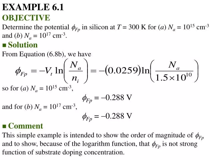
EXAMPLE 6.1 • OBJECTIVE • Determine the potential Fp in silicon at T = 300 K for (a) Na = 1015 cm-3 and (b) Na = 1017 cm-3. • Solution From Equation (6.8b), we have so for (a) Na = 1015 cm-3, Fp= 0.288 V and for (b) Na = 1017 cm-3, Fp= 0.288 V • Comment • This simple example is intended to show the order of magnitude of Fp and to show, because of the logarithm function, that Fp is not strong function of substrate doping concentration.
EXAMPLE 6.2 • OBJECTIVE • Calculate the maximum space charge width given a particular semiconductor doping concentration. • Consider silicon atT = 300 K doped to Na = 1016 cm-3. • Solution From Equation (6.8b), we have Then the maximum space charge width is or xdT= 0.30 10-4 = 0.30 m • Comment • The maximum induced space charge width is on the same order of magnitude as pn junction space charge widths.
EXAMPLE 6.3 • OBJECTIVE • Calculate the metal-semiconductor work function difference ms for a given MOS system and semiconductor doping. • For an aluminum-silicon dioxide junction, m = 3.20 V and for a silicon-silicon dioxide junction, = 3.25 V. We can assume that Eg = 1.12 eV. Let the p-type doping be Na = 1014 cm-3. • Solution For silicon at T = 300 K, we can calculate Fp as Then the work function difference is or ms = -0.838 V • Comment • The value of ms will become more negative as the doping of the p-type substrate increases.
EXAMPLE 6.4 • OBJECTIVE • Calculate the flat-band voltage for a MOS capacitor with a p-type semiconductor substrate. • Consider an MOS structure with a p-type semiconductor substrate doped to Na = 1016 cm-3, a silicon dioxide insulator with a thickness of tox = 500Ǻ, and an n+ polysilicon gate. Assume that Qss =1011 electronic charges per cm2. • Solution The work function difference, from Figure 6.21, is ms = 1.1 V. The oxide capacitance can be found as The equivalent oxide surface charge density is Qss = (1011)(1.6 10-19)= 1.6 10-8 C/cm2 The flat-band voltage is then calculated as • Comment • The applied gate voltage required to achieve the flat-band condition for this p-type substrate is negative. If the amount of fixed oxide charge increases, the flat-band voltage becomes even more negative.
EXAMPLE 6.5 • OBJECTIVE • Design the oxide thickness of an MOS system to yield a specified threshold voltage. • Consider an n+ polysilicon gate and a p-type silicon substrate doped to Na = 5 1016 cm-3. Assume Qss = 1011 cm-2. Determine the oxide thickness such that VTN = + 0.40 V. • Solution • From Figure 6.21, the work function difference is ms 1.15 V. The other various parameters can be calculated as • and • Then • QSD(max) = eNaxdT = (1.6 10-19)(5 1016)(0.142 10-4) • or • QSD(max) = 1.14 10-17 C/cm2
EXAMPLE 6.5 • Solution The oxide thickness can be determined from the threshold equation Then which yields tox = 272 Ǻ • Comment • The threshold voltage for this case is a positive quantity, which means that the MOS device is an enhancement-mode device; a gate voltage must be applied to create the inversion layer charge, which is zero for zero applied gate voltage.
EXAMPLE 6.6 • OBJECTIVE • Calculate the threshold voltage of an MOS system using an aluminum gate. • Consider a p-type silicon substrate at T = 300 K doped to Na = 1014 cm-3. Let Qss = 1010 cm-2, tox = 500 Ǻ, and assume the oxide is silicon dioxide. From Figure 6.21, we have that ms = 0.83 V. • Solution We can start calculating the various parameters as and Then • QSD(max) = eNaxdT = (1.6 10-19)(1014)(2.43 10-4) = 3.89 10-9 = 3.89 10-9 C/cm2
EXAMPLE 6.6 • Solution We can now calculate the threshold voltage as • Comment • In this example, the semiconductor is very lightly doped, which, in conjunction with the positive charge in the oxide and the work function potential difference, is sufficient to induce an electron inversion layer charge even with zero applied gate voltage. This condition makes the threshold voltage negative.
EXAMPLE 6.7 • OBJECTIVE • Design the semiconductor doping concentration to yield a specified threshold voltage. • Consider an aluminum-silicon dioxide-silicon MOS structure. The silicon is n type, the oxide thickness is tox = 500 Ǻ, and the trapped charge density is Qss = 1010 cm-2. Determine the doping concentration such that VTP = 1.0 V. • Solution The solution to this design problem is not straightforward, since the doping concentration appears in the terms Fn , xdT , QSD(max), and ms . The threshold voltage, then, is a nonlinear function of Nd . Without a computer-generated solution, we resort to trial and error. For Nd = 2.5 1014 cm-3, we find and Then • QSD(max) = eNaxdT = 6.48 10-9 C/cm2
EXAMPLE 6.7 • Solution From Figure 6.21, ms = 0.35 V the threshold voltage is which yields VTP = -1.006 V and is essentially equal to the desired result. • Comment • The threshold voltage is negative, implying that this MOS capacitor, with the n-type substrate, is an enhancement mode device. The inversion layer charge is zero with zero gate voltage, and a negative gate voltage must be applied to induce the hole inversion layer.
EXAMPLE 6.8 • OBJECTIVE • Calculate the electric field in and the voltage across the oxide at a flat-band condition. • Assume that Qss = 8 1010 cm-2 in silicon dioxide and assume the oxide thickness is tox = 500 Ǻ. • Solution The electric charge density at the interface is Qss = (1.6 10-19)(8 1010) = 1.28 10-8 C/cm2 The oxide electric field is then Since the electric field across the oxide is a constant, the voltage across the oxide is then Vox = oxtox = (3.71 104) (150 10-8 or Vox = 55.6 mV • Comment • In the flat-band condition, an electric field exists in the oxide and a voltage exists across the oxide due to the Qss charge.
EXAMPLE 6.9 • OBJECTIVE • Calculate Cox , Cmin , and CFB for an MOS capacitor. • Consider a p-type silicon substrate at T = 300 K doped to Na = 1016 cm-3. The oxide is silicon dioxide with a thickness of 500 Ǻ and the gate is aluminum. • Solution The oxide capacitance is To find the minimum capacitance, we need to calculate and
EXAMPLE 6.9 • Solution Then We can note that The flat-band capacitance is We can also note that • Comment • The ratios of Cmin to Cox and of CFB to Cox are typical values obtained in C – V plots.
EXAMPLE 6.10 • OBJECTIVE • Design the width of a MOSFET such that a specified current is induced for a given applied bias. • Consider an ideal n-channel MOSFET with parameters L = 1.25 m, n = 650 cm2/V-s, Cox = 6.9 10-8 F/cm2, and VT = 0.65 V. Design the channel width W such that ID(sat) = 4 mA for VGS = 5 V. • Solution We have, from Equations (6.51) and (6.52), or Then W = 11.8 m • Comment • The current capability of a MOSFET is directly proportional to the channel width W. The current handling capability can be increased by increasing W.
EXAMPLE 6.11 • OBJECTIVE • Determine the inversion carrier mobility from experimental results. • Consider an n-channel MOSFET with W = 15 m, L = 2 m, andCox = 6.9 10-8 F/cm2. Assume that the drain current in the nonsaturation region for VDS = 0.10 V is ID = 35 A at VGS = 1.5 V and ID = 75 A at VGS = 2.5 V. • Solution From Equation (6.58), we can write so that which yields n = 773 cm2/V-s • Comment • The mobility of carriers in the inversion layer is less than that in the bulk semiconductor due to the surface scattering effect. We will discuss this effect in the next chapter.
EXAMPLE 6.12 • OBJECTIVE • Determine the conduction parameter and current in a p-channel MOSFET. • Consider a p-channel MOSFET with parameters p = 300 cm2/V-s, Cox = 6.9 10-8 F/cm2, (W/L) = 10, and VTP = -0.65 V. Determine the conduction parameter Kp and find the maximum current at VSG = 3 V. • Solution We have The maximum current occurs when the transistor is biased in the saturation region, or ID = Kp(VSG + VTP)2 = 0.104[3 + (-0.65)]2 = 0.574 mA • Comment • The conduction parameter, for a given width-to-length ratio, of a p-channel MOSFET is approximately one-half that of an n-channel MOSFET because of the reduced hole mobility value.
EXAMPLE 6.13 • OBJECTIVE • Calculate the change in the threshold voltage due to an applied source-to-body voltage. • Consider an n-channel silicon MOSFET at T = 300 K. Assume the substrate is doped to Na = 3 1016 cm-3 and assume the oxide is silicon dioxide with a thickness of tox = 500 Ǻ. Let VSB = 1 V. • Solution We can calculate that We can also find Then from Equation (6.87), we can obtain or VT = 1.445(1.324-0.867) = 0.66 V • Comment • Figure 6.64 shows plots of versus VGS for various values of applied VSB. The original threshold voltage, VT0 , is 0.64 V.
EXAMPLE 6.14 • OBJECTIVE • Calculate the cutoff frequency of an ideal MOSFET with a constant mobility. • Assume that the electron mobility in an n-channel device is n = 400 cm2/V-s and that the channel length is L = 1.2m. Also assume that VTN = 0.5 V and let VGS = 2.2 V. • Solution From Equation (6.103), the cutoff frequency is • Comment • In an actual MOSFET, the effect of parasitic capacitance will substantially reduce the cutoff frequency from that calculated in this example.
