Hard drive
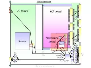
Electronics placement. 9U board. 6U board. VME. TTL driver. Hard drive. VME. mezzanine board. EPROM. TTL driver. PCI. AMCC S5935 PQFP 160. TTL drivers. Control signals. Add-on. EIDE. ECL drivers. Magic bus. Display. clk40MHz. EPROM. Altera APEX 20K200 Fineline BGA 484.

Hard drive
E N D
Presentation Transcript
Electronics placement 9U board 6U board VME TTL driver Hard drive VME mezzanine board EPROM TTL driver PCI AMCC S5935 PQFP 160 TTL drivers Control signals Add-on EIDE ECL drivers Magic bus Display clk40MHz EPROM Altera APEX 20K200 Fineline BGA 484 FIFOs The proportions of the boards are respected
DSD[15:0] DRST_L DMARQ0 DIOW_L DIOR_L DCHRDY DMACK0_L IDE DIRQ1 DIOCS16 DSA1 DSA0 31 signals DSA2 DCS0_L DCS1_L HD_ACT_P_L adapt
P1 GAP* MBDATA[127:0] 6 signals MBAD[31:0] GA[4:0]* MB_BUFFER[1:0] MOD_DONE[18:0] P3 EV_LOADED*[3:0] MB_MBRESET P0 BOSS MB_AP_FIFO_EMPTY 0 signal MB_RD_WR* 196 signals MB_START_LOAD MB_DSTROBE BOSS_REQ DONE_OUT P2 CDF_CLK MB_DDONE* CDF_CLK* BOSSGROUT CDF_BC* BOSSGRIN CDF_B0* CDF_L1A* 46 signals CDF_L1R* CDF_L2B[1:0]* CDF_HALT* CDF_RECOVER* CDF_ABORT* CDF_CALIB[6:0]* D0_IO_P2[7:0] CDF_ERROR_P2* CDF_L2A* 248 signals CDF_L2BD[1:0]* CDF_GLIVE* L1_CALIB* RSVD_L1W2* CDF_STOP* CDF_TEST* CDF_RUN* CDF_RL[2:0]* CDF_CALEN* CDF_L2R* CDF_L2A_EN* CDF_EVID[3:0]*
TSI connector ECL drivers TSI_IN[15:0] TSI_PINS[63:0] TSI_OUT[15:0] 64 signals 32 signals
DQ[31:0] BP_CLK IRQ* SYSRST* ADR[6:2] Add-on bus BE[3:0]* SELECT* WR* RD* PT_NUM[1:0] PTBE[3:0]* PTATN* PTBURST* 62 signals PTADR* PTWR PTRDY* WRFULL WRFIFO* RDEMPTY RDFIFO*
TTL drivers MB 32 AMCC 128 FIFO 32 Add-on 128 Altera Simplest diagram, but cannot allow a 64kB FIFO -> not recommended
First diagram planned, allows the MB to read back the FIFO (with no risk of collision with the Add-on bus) TTL drivers MB 32 AMCC 128 128 FIFO 32 Altera Add-on 128
Simplified diagram, the FIFO is directly read by the Add-on bus The MB can still read the FIFO, but only for testing purposes ( risk of collision with the Add-on bus) We save 32 pins on the Altera -> sound solution ! TTL drivers MB 32 AMCC 128 128 32 FIFO 32 Altera Add-on 128
FPGA details count of the pins with this last architecture Control signals from P1 and P2 connectors Add-on bus 62 52 ??? 4 Altera APEX 20K200 Fineline BGA 484 Switches 15 test points --1-- Clock 5 TTL drivers control signals Total : 376 signals out of 376 available (15 spare signals -> test points) 5 Display 23.2 mm 196 Magic bus --5-- EPROM 5 FIFOs control signals 32 ECL drivers 23.2 mm height : 1.86 mm the geometry of the input/output pins is not respected