EDX
EDX . E nergy D isperse X analysis. Bolesław AUGUSTYNIAK. SEM. TEM. Electron-Atom Interaction. EDX – basics (1).

EDX
E N D
Presentation Transcript
EDX Energy Disperse X analysis Bolesław AUGUSTYNIAK
SEM TEM Electron-Atom Interaction
EDX – basics (1) Energy depressive x-ray spectroscopy (EDX or EDS) is a chemical microanalysis technique performed in conjunction with a scanning electron microscope (SEM). The technique utilizes x-rays that are emitted from the sample during bombardment by the electron beam to characterize the elemental composition of the analysed volume. Features or phases as small as about 1µm can be analysed.
EDX – basics (2) When the sample is bombarded by the electron beam of the SEM, electrons are ejected from the atoms comprising the sample's surface. A resulting electron vacancy is filled by an electron from a higher shell, and an x-ray is emitted to balance the energy difference between the two electrons. The EDS x-ray detector measures the number of emitted x-rays versus their energy. The energy of the x-ray is characteristic of the element from which the x-ray was emitted. A spectrum of the energy versus relative counts of the detected x-rays is obtained and evaluated for qualitative and quantitative determinations of the elements present in the sampled volume. http://www.mee-inc.com/eds.html#x-rays
EDX - detector X-ray photons from the sample pass through a thin window isolating the specimen chamber environment from the detector into a cooled, reverse-bias p-i-n Si(Li)crystal. Absorption of each individual x-ray photon leads to the ejection of a photoelectron, which gives up most of its energy to the formation of electron-hole pairs. They are swept away by the applied bias to form a charge pulse, which is then converted into a voltage pulse by a charge-to-voltage converter. The signal is further amplified and shaped by a linear amplifier and finally passed to a computer x-ray analyzer, where the data are displayed. The key to understanding how an EDX works is to recognize that each voltage pulse is proportional to the energy of the incoming x-ray photon. http://www.phys-astro.sonoma.edu/people/faculty/shi/P466/lecture6.doc
Si(Li) detectorefficiency • Characteristics High voltage : - 500 V polarization : Negative Cooling : liquid N2 in a Dewar (to be filled twice a week) Window : 8 microns thick beryllium • surface = 12 mm2 aperture diameter = 4 mm sensitive layer thickness = 4.2 mm The Si(Li) detector is a solid-state semiconductor detector used for X-ray fluorescence analysis. The spectrum is read out on a Multichannel Analyzer over 512 to 8192 channels. http://www.esrf.fr/UsersAndScience/Experiments/Imaging/ID22/BeamlineManual/Detectors/SiLi
Si(Li) detector(2) Detection Efficiency vs. Be Window Thickness Low-Energy Curve and vs. Crystal Thickness on High-Energy Curve ORTEC SLP Series Lithium-Drifted Silicon X-Ray Detectors The energy range of detection is from 30 keV down to 1 keV, depending on the thickness of the beryllium window. The x-ray detector consists of a lithium-drifted silicon crystal and a cryogenically-cooled-FET, a high-gain, low-noise hybridized preamplifier in a PopTop capsule with a thin Be entrance window http://www.ortec-online.com/detectors/photon/b2_4_6.htm
EDX applications • Surface contamination analysis • Corrosion evaluations • Coating composition analysis • Rapid material alloy identification • Small component material analysis • Phase identification and distribution
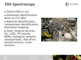
EDX – analyser Structural and chemical analyser for SEM http://www.renishaw.com/client/product/UKEnglish/PGP-1078.shtml The instrument is outfitted with a Link Analytical pentafet SiLi energy-dispersive x-ray spectrometer which has a turret control that allows either a Beryllium window or a Boron Carbide window to be used for normal or light element x-ray acquisition, respectively. http://www.geo.arizona.edu/tectonics/Ducea/methods/SEM.html
Przykłady widma EDX http://www.mee-inc.com/eds1.html
Przykłady widma EDX (2) EDX Spectrum for contamination on stainless steel mesh. http://www.mee-inc.com/eds1.html
EDX line profile http://www.mee-inc.com/eds1.html
Wyniki analizy X-widma The backscattered image of the sample is shown in the bottom left image pane. The lines indicate the distribution of copper (green), sulphur (red) and silicon (white) as measured across the horizontal scan line. X-ray maps of the sample reveal the spatial distribution of (clockwise from top left); silicon, copper and sulphur. http://www.rmcs.cranfield.ac.uk/dmms/cmse/electronmicrographs
Wyniki analizy EDX Elemental map of polished metallographic cross-section of high-chromium white-iron casting. http://www.mee-inc.com/eds1.html
Wyniki analizy EDX (2) The small spheres are inclusions in a fractured steel sample. Manganese and sulphur were detected by spot EDS analysis of one of the spheres (see the EDS spectrum below). MnS and MnS2 inclusions are common in certain steels but although EDS allows us to identify the elemental composition of inclusions we cannot be certain of the chemical composition. The spectrum was used to identify the elements Mn, S and Fe. The Mn and S are from the sphere; the Fe is probably detected because of scattering of the electron beam into the surrounding steel. http://www.rmcs.cranfield.ac.uk/dmms/cmse/electronmicrographs
Sample 347 p1, external wall, EDXNi distribution Sample 347 p1, external wall, EDX Cr distribution Sample 347 p1, external wall, SEM picture Sample 347 p1, external wall, EDX O distribution Sample 347 p1, external wall, EDX Nb distribution Sample 347 p1, external wall, EDX Fe distribution
deposit area at interface layer bulk material
Zalety EDX • Electron microscopic analysis of elements provides some advantages compared to wet chemical analysis: • - X-ray sampling is non-destructive • - natural heterogeneity is retained • - analysis can be conducted on microgram quanitities • - adjacent structures can be directly compared • - excellent probe size (20 to 200 nanometers) http://www.ou.edu/research/electron/element.html