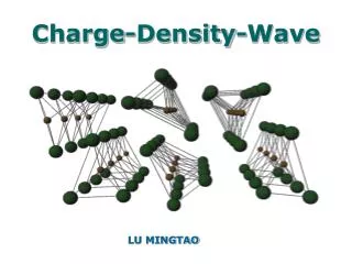
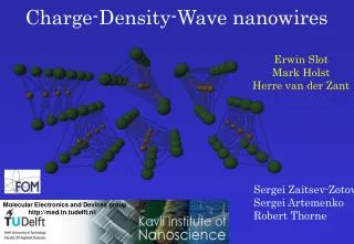
Charge-Density-Wave nanowires
Charge-Density-Wave nanowires. Erwin Slot Mark Holst Herre van der Zant. Sergei Zaitsev-Zotov Sergei Artemenko Robert Thorne. Molecular Electronics and Devices group. http://med.tn.tudelft.nl/. 3 m m. 1 m m. 5 m m. submicron CDW devices. etched wires in crystals. nanowires.

Charge-Density-Wave nanowires
E N D
Presentation Transcript
Charge-Density-Wave nanowires Erwin Slot Mark Holst Herre van der Zant Sergei Zaitsev-Zotov Sergei Artemenko Robert Thorne Molecular Electronics and Devices group http://med.tn.tudelft.nl/
3 mm 1 mm 5 mm submicron CDW devices etched wires in crystals nanowires thin films junctions/constrictions 5mm submicron probes bulk CDW properties studied in detail; much less in known about the microscopic details
Nb Se II III I multi-chain nanowires NbSe3 wires Ultrasonic cleaving in pyridine Disperse on substrate with predefined markers
1 mm contacting nanowires 2 mm E-beam lithography Buffered Hydrofluoric acid (4 sec) Deposition of Ti and Au width: 30-300 nm, thickness: 10-50 nm Lowest contact resistance ~100 W
linear resistance measurements power-law behavior E. Slot et al. Phys. Rev. Lett. 93 (2004) 176602 reducing cross section 1D CDW dynamics E. Slot et al., Phys. Rev. B 69 (2004)
ET -ET sliding pinned sliding 10-3mm2 3 x 10⁻³mm2 7 x 10⁻³mm2 22 x 10-3mm2 threshold field increases as cross section decreases T=120 K
1D collective pinning: single phase coherent domain 2D 1D slope 2/3 evidence of 1D weak collective CDW pinning: ET (1/A)2/3 slope 1/2 surface and 2D pinning with ET (1/A)1/2 can be excluded E. Slot et al., Phys. Rev. B 69 (2004)
no evidence for single-particle model in IV characteristics ET -ET sliding pinned sliding 10-3mm2 3 x 10⁻³mm2 7 x 10⁻³mm2 single-particle expectation 22 x 10-3mm2 T=120 K
gradual reduction of transition temperatures as cross section decreases R/L (kW/mm) R/L (kW/mm)
R T-a power-law behavior in R(T)
power-law behavior in I-V(T) R T-a: a = 2.15 I Vb : b = 4.2 I/Ta+1 = C sinh(geV/kBT) |G(1+b/2+igeV/pkBT)|2 power-law in both I(V) and R(T), and scaling behavior (bosonic excitations with linear spectrum) are a fingerprint for 1D transport
power-law behavior due to uncondensed carriers ! coexistence of power law behavior and sliding threshold in IVs no abrupt decrease of nonzero TP1,TP2 R/L (kW/mm) R/L (kW/mm)
multiwall carbon nanotubes Bachtold et al., Phys. Rev. Lett. 87, 166801 (2001)
and NbSe3 MWNT • Both diffusive conductors • Both interaction between chains • Both show power-law behaviour • Both show scaling of I(V)s Xinluo Zhao et al., Phys. Rev. Lett. 90, 187401 (2003) 7 Å 7 Å LL and ECBT have the same dependencies on energy
Environmental Coulomb Blockade Ingold & Nazarov, Single charge tunneling Matveev & Glazman, Phys. Rev. Lett. 70, 990 (1993) Coulomb blockade is smeared by quantum fluctuations in the leads ‘Environment’ (Z-transmission line) I(V) Vb b = 2Z/RQ + 1 V Junction
nanowire as transmission line R’ L’ G’ C’ V For NbSe3 nanowire: Kinetic inductance L’ = 17 nH/mm (very high!) Capacitance C’ = 10 aF/mm Z = 41 kW 1.6RQ
nanowire with tunnel barrier LC V wL’ > R’ ħ> 0.4 meV measurement I(V) Vb b = 2Z/RQ + 1 4.2 model b = 4.2 Z = 41 kW 1.6RQ
model reproduces dependence of exponentsof R(T) on cross section
‘Environment’ V Junction low carrier density (1018 cm-3: 30 nm distance between electrons) and low Fermi energy indicate the importance of e-e interactions Environmental Coulomb Blockade But applicability of ECB is not clear: developed for a single junction • Alternative model: Wigner crystal • Coulomb energy larger than Fermi energy • Power-law exponent determined by localization length Data in agreement with general concepts describing 1D conductors. At present no full theory describing our system with many channels and disorder.
gate effect: periodic features are NOT observed switches occur with pulses on the gate IVs are switchy when the gate is not grounded
Conclusions • As the cross-section of CDW nanowires becomes smaller, the Peierls temperature gradually decreases and the threshold field increases (1D collective pinning) • Below TP2: NbSe3 nanowires with less than 1000 chains in total show power-law behavior typical for 1D transport • Data in agreement with general concepts describing 1D • conductors. At present no full theory describing our • system with many channels and disorder • Role of impurities: discussed by Artemenko on Monday
conclusions • Current conversion occurs through strain-induced phase-slip processes (changes on the micron scale) • Importance of strain: change in the chemical potential (negative resistance) • Energy spectroscopy in CDW junctions and weak links: evidence for solitons • A single phase coherent CDW domain can not be described with the single particle model • Thin NbSe3 nanowires show the characteristics of one-dimensional transport (power-law behavior; low electron density) • A full microscopic CDW model needed
gradual reduction of transition temperatures as cross section decreases bulk sample
1D collective pinning Fukuyama-Lee-Rice Hamiltonian: 3D Weak pinning 1D Weak pinning ET independent on size ET (1/A)2/3