Simulation study and tool development for ultra-scaled InAs HEMTs Theme 6
10 likes | 179 Vues
Simulation study and tool development for ultra-scaled InAs HEMTs Theme 6. 2015-2019 Research. L g. Gate. Φ M. m y ins. InAlAs. Source. t ins. m y buf. InGaAs. Drain. Fitted to tight-binding bandstructure. m y. m x,z. Strained InAs.

Simulation study and tool development for ultra-scaled InAs HEMTs Theme 6
E N D
Presentation Transcript
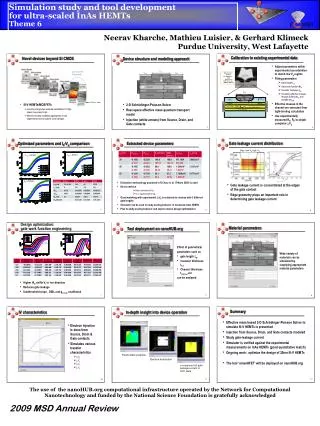
Simulation study and tool development for ultra-scaled InAs HEMTsTheme 6 2015-2019 Research Lg Gate ΦM myins InAlAs Source tins mybuf InGaAs Drain Fitted to tight-binding bandstructure my mx,z Strained InAs Neerav Kharche, Mathieu Luisier, & Gerhard Klimeck Purdue University, West Lafayette Calibration to existing experimental data Novel devices beyond Si CMOS Device structure and modeling approach • Adjust parameters within experimental uncertainties to match low Vg regime • Fitting parameters • Gate length Lg • Gate work function Φm • Insulator thickness tins • Tunneling effective masses through InAlAs myox and InGaAs mybuff • Effective masses in the channel are extracted from tight-binding calculation • Use experimentally measured RS, RD to obtain complete Id-Vg Experimental Devices: III-V HEMTs for Logic Applications (D.H. Kim et. al, IEDM 07, EDL 08) Robert Chau, Intel • 2-D Schrödinger-Poisson Solver • Real-space effective mass quantum transport model • Injection (white arrows) from Source, Drain, and Gate contacts • III-V HEMTs/MOSFETs • recently emerged as potential candidates for high-speed, low-power logic • Need to develop modeling approaches to aid experiments and to explore novel designs 1 2 3 Gate leakage current distribution Extracted device parameters Optimized parameters and Id-Vg comparison Bias: low Vg high Vd Lg = 40nm Lg = 30nm Lg = 50nm • Evaluation methodology proposed in R.Chau et. al. (T-Nano 2005) is used • Device metrics • Black: simulated Id-Vg • Red: experimental Id-Vg • Good matching with experimental Id-Vg is achieved for devices with 3 different gate lengths • Simulator can be used to study scaling behavior of nanoscale InAs HEMTs • Plan to study scaling behavior and explore device design optimizations • Gate leakage current is concentrated at the edges of the gate contact • Edge geometry plays an important role in determining gate leakage current 4 5 6 Design optimization: gate work function engineering Material parameters Tool deployment on nanoHUB.org Vd=0.5V Vd=0.05V Effect of geometrical parameters such as • gate length Lg, • insulator thickness tins, • Channel thickness tchannel etc can be analyzed Wide variety of materials can be simulated by supplying appropriate material parameters • Higher Φm shifts Vt in +ve direction • Reduces gate leakage • Subthreshold slope , DIBL and gm,max unaffected 8 7 9 Summary IV characteristics In-depth insight into device operation • Effective mass based 2-D Schrödinger-Poisson Solver to simulate III-V HEMTs is presented • Injection from Source, Drain, and Gate contacts modeled • Study gate-leakage current • Simulator is verified against the experimental measurements on InAs HEMTs (good quantitative match) • Ongoing work: optimize the design of 20nm III-V HEMTs • The tool ‘omenHFET’ will be deployed on nanoHUB.org • Electron injection is done from Source, Drain & Gate contacts • Simulates various transfer characteristics • Id-Vg • Ig-Vg • Id-Vd • Ig-Vd Electrostatic potential Electron distribution y-component of gate leakage current in OFF state 12 11 10 The use of the nanoHUB.org computational infrastructure operated by the Network for Computational Nanotechnology and funded by the National Science Foundation is gratefully acknowledged 2009 MSD Annual Review