Intrinsic semiconductor
Intrinsic semiconductor. Doped semiconductor N-type. Doped semiconductor P-type. Electric current in semiconductors. Drift of charged carriers. Electric current in semiconductors. J p,drift = q μ p pE J n,drift = q μ n nE. v d = μ p E. I p,drift = qpv d A.
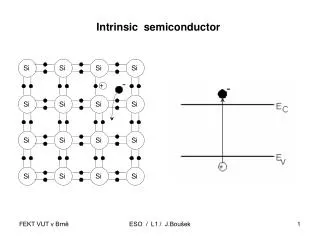

Intrinsic semiconductor
E N D
Presentation Transcript
Intrinsic semiconductor ESO / L1 / J.Boušek
Doped semiconductor N-type ESO / L1 / J.Boušek
Doped semiconductor P-type ESO / L1 / J.Boušek
Electric current in semiconductors Drift of charged carriers ESO / L2 / J.Boušek
Electric current in semiconductors Jp,drift = qμppE Jn,drift = qμnnE vd = μpE Ip,drift = qpvd A Jp,drift = qpvd ESO / L2 / J.Boušek
Dependence on dopant concentration ESO / L2 / J.Boušek
Diffusion ESO / L2 / J.Boušek
Diffusion 1. Fick-Law: ESO / L2 / J.Boušek
Diffusion + Drift Einstein equation ESO / L2 / J.Boušek
Generation and recombination • Generation = need energy = generation in pairs: (electron + hole) • - photo-generation • - thermal excitation of the crystal lattice • - high energy electron • Recombination = loss of energy = recombination in pairs: (el. + hole) : • - large number of complicated processes - direct (interband) - undirect (recombination centres, traps) - surface • generation lifetime recombination • electrones… n holes…. p ESO / L2 / J.Boušek
Lifetime of the carriers Doped semiconductor: Type N n >> p ; Type P p >> n Usually : n , p ≈ 1 s High quality silicon : n , p ≥ 1 ms High density of traps / of recombination centres : n , p ≈ 1 s ÷1 ns - High speed devices: Intentionally ... Au (Al) - Low quality production: Crystal distortions, Impurities ESO / L2 / J.Boušek
Thermal equilibrium p0 n0 = ni2equilibrium state (index "0") Distortion of thermal equilibrium: n = n0 +n ; p = p0 +p (n a pconcentration of non-equilibrium carriers) Injection : np > ni2 low(n << n0) - medium (n n0) - high (n >> n0) Extraction : np < ni2. ESO / L2 / J.Boušek
PN-Junction in equilibrium state Depletion region ESO / L2 / J.Boušek
PN-Junction in equilibrium state Concentration of dopants: ND = 1019 m-3 NA = 1020 m-3 Electrons in N: nn = ND = 1019 m-3 Electrons in P: np = ni2 / NA = 1032 m-6 / 1020 m-3 =1012 m-3 Difference in concentration 107 electron diffusion to P !!!!! In N only ionized donors (ND +) standing firmly in the lattice Holes in P: pp = NA = 1020 m-3 Holes in N: pp = ni2 / ND = 1032 m-6 / 1019 m-3 =1013 m-3 Difference in concentration 107 diffusion of holes to N !!!!! In N only ionized donors (ND +) standing firmly in the lattice Ionized dopants create space charge !!!!!!!!! ESO / L2 / J.Boušek
Space charge in depletion area Electrical field Potential ESO / L2 / J.Boušek
PN-Junction in equilibrium state Density of the space charge given by dopants concentration Junction area with lower dopants concentration ís wider Consequence : Electrical field in depletion area Emax- in metalurgical junction !!!! Potential difference between P and N : Diffusion voltage. Actual potential value given by the shape of electrical field ESO / L2 / J.Boušek
Band-diagram of PN-Junction ESO / L2 / J.Boušek
Band-diagram of PN-Junction 1) The position of EF in both areas P and N must correspond to the type of semiconductor / type of conductivity. (shift EF to EV in case of “P-type“ or to EC in case of “N-type“) 2) In Thermal equilibrium the value of Fermi level EF is constant. To fulfuill both 1) + 2) : a) mutual shift of Conductive and Valence bands (band-bending) b) The shift corresponds to qUD . qUD : energetic treshold - prevents diffusion of majority carriers. ESO / L2 / J.Boušek
PN junction in FORWARD polarisation Diffusionvoltage - barrieragainstdiffusionof majority carriers Equilibriumstate : Onlysmalldiffusioncurrentwhichiscompensatedwiththe drift casused by potentialdifference in spacecharge area. majority carriers - diffusion minoritní carriers - drift In forward polarisation : external voltage acts against the potential in depletion area - the barrier / treshold is lower !!! Forward current is made by DIFFUSSION of majority carriers !! ESO / L2 / J.Boušek
PN junction in REVERSE polarisation • Polarity of external voltage is the same as the polarity of electrical field in the space charge region: • !! Electrical field in the space charge region grows !! • Electrical field in space charge region enhance the drift of minority carriers from quasineutral parts of the junction: • The concentration of minority carriers in quasineutral parts of the junction drops. • When increasing the reverse voltage the reverse current does not increase !!!! Reverse current : DRIFT current of minority carriers !!!! ESO / L2 / J.Boušek