Understanding Silicon Doping and Junctions in Transistors
260 likes | 475 Vues
Learn about intrinsic and extrinsic silicon characteristics, doping concentrations, pn junction, MOS transistor structure, operation regimes, threshold voltage, and ion implantation. Explore numerical examples and threshold adjustment methods.

Understanding Silicon Doping and Junctions in Transistors
E N D
Presentation Transcript
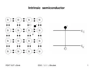
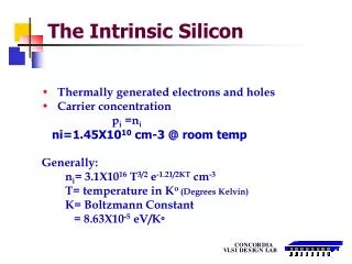
The Intrinsic Silicon • Thermally generated electrons and holes • Carrier concentration • pi =ni • ni=1.45X1010 cm-3 @ room temp • Generally: • ni= 3.1X10¹⁶ T3/2 e-1.21/2KT cm-3 • T= temperature in Ko (Degrees Kelvin) • K= Boltzmann Constant • = 8.63X10⁻⁵ eV/Ko
The Extrinsic Silicon Number of carriers is increased by introducing foreign atoms called impurities The process of introducing impurities is called doping Two Types of dopants: p type and n type p-type dopants: Boron (B), Gallium (G), Aluminum (Al) n-type dopants: Arsenics (Ar), Phosphorous (P), Antimony (Sb)
Doping Concentration P-type: concentration = p = NA+pth NA= concentration of p type do pant (atoms/cm3) pth= concentration of thermally generated holes (holes/cm3) p NA (NA>> pth ) n-type: concentration = n = ND+nth ND= concentration of n type do pant (atoms/cm3) nth= concentration of thermally generated electrons (electrons/cm3) n ND (ND>> nth )
Degrees of Doping • Degree of concentration • N- - or P - - : ND or NA<1014 cm-3 • N- or P - : 1014 cm-3 <ND or NA<1016 cm-3 (lightly doped) • N or P : 1016 cm-3<ND or NA<1018 cm-3 (moderately doped) • N+ or P + : 1018 cm-3<ND or NA<1020 cm-3 (heavily doped) • N++ or P ++ : ND or NA>1020 cm-3
Review of the pn Junction p type Depletion Region n type Potential across pn junction: D = (KT/q) ln( NA.ND/ni2 ) Depletion) region length: Xd = K [ [ (1/NA) + (1/ND)] D ]0.5 K constant a function of ( εsi , q ) D P- N+ Junction Capacitance: Cj = Cjo / (1+V/ D)0.5 It is a function of the applied voltage and doping concentration P+ N- Xd
Vg Gate Metal Insulator Sio2 P+ Substrate vB Two terminal MOS Structure Depth of Depletion region: Xd = { 2 εSi . |s - F │ }0.5 The Charge Density: Q = - { 2 q NAεSi . |s - F │ }0.5
Cross-section of pn -junction in an IC process The Physical Structure Al SiO 2 N+ P+ n n P+ Al Al
Nmos Transistor D Polycrystalline silicon G Gate Gate oxide S Enhancement NMOS D (Bulk) G B S NMOS with Bulk Contact
Gate oxide Polysilicon Gate Al Al SiO2 SiO2 SiO2 S D Field Oxide Field Oxide n+ channel n+ L P Substrate contact Metal (G) L (S) (D) n+ n+ W Poly The Physical Structure (NMOS) The process and sequence is designed by the fabrication house You design the MASKS
G S D N+ N+ -Ve charge -Ve charge p-type G S D p-type G S D p-type Regimes of Operation 1. Accumulation VGS is negative Majority carries attracted to the surface 2. Depletion VGS increased by a small amount Majority carriers depleted Space charge (depletion) region formed 3. Inversion VGS increased further Minority carriers attracted to surface Inverted surface provides conduction Inverted surface to N-type
The Threshold Voltage • The voltage applied between the gate and the source which causes the beginning of the channel surface strong inversion. • Threshold voltage Vt is a function of: • Vfb = flatband voltage; depends on difference in work function between gate and substrate and on fixed surface charge. • Fs = surface potential. • Gate oxide thickness. • Charge in the channel area. • Additional ion implantation. • Typical values: 0.2V to 1.0V for NMOS and -0.2 to -1.0V for PMOS
D G B VSB S Threshold Adjust • Threshold voltage is a function of source to substrate voltage VSB. • Body factor is the coefficient for the VSB dependence factor. , Φs =2ΦF Fs is the surface potential ~ -0.6V for NMOS is the body factor ~ 0.6 to 1.2 V1/2 Fermi potential ΦF is is –ve in nMOS, +ve in pMOS The body effect coefficient γ is +ve in nMOS, -ve in pMOS The substrate bias voltage VSB is +ve in nMOS, -ve in pMOS
Ion Implantation (dopant) S D channel p Substrate Threshold Adjust • nMOS transistors implanted with n-type dopant results in a decrease in threshold voltage • An effective mean to adjust the threshold is to change the doping concentration through an ion implantation dose. • nMOS transistors implanted with p-type dopant results in an increase in the threshold voltage. VTO’=VTO + (q . DI /Cox) DI = dose of dopant in the channel area(atoms/cm2) Cox = gate oxide capacitance per unit area
Threshold Adjust… Continued Example of Numerical Values for our process
D G S Depletion NMOS Al n+ n+ n+ n+ P+ P+ Threshold Adjust • Depletion NMOS transistor • Heavy ion implantation of n dopant in the channel area results in negative threshold voltage • Transistor conducts with zero gate to source voltage. • It is called Depletion mode transistor • Field threshold adjust • Required to minimize interaction between transistors. • Heavy implantation called p-guard/n-guard • VTF = 12 to 22V P+
V V GS DS S I G D D + + n n p -substrate Current-Voltage Relations MOS transistor and its bias conditions
gate source channel drain Id Gate Voltage and the Channel VGS > VT VDS< (VGS-VT) gate VGS > VT VDS = (VGS –VT ) source drain Id gate VGS > VT VDS > (VGS-VT ) source drain Id
Qualitative Operation of NMOS Transistor • 1. Cut-Off Region • VGS < VT • No Inversion or Weak Inversion • IDS = leakage current or sub-threshold current • 2. Linear Region • VGS > VT and VDS<VGS-VT • Channel surface is inverted • Output current depends on VGS and VDS • The relationship between IDS and VDS is almost linear
NMOS Operation-Linear Process Tranconductance uA/V2 for 0.35u, K’ (Kp)=196uA/ V2 Gate oxide capacitance per unit area eox = 3.9 x eo = 3.45 x 10⁻¹¹ F/m tox Oxide thickness for 0.35 u and tox=100Ao Quick calculation of Cox: Cox= 0.345 / tox (Ao) pf/um2 u = mobility of electrons 550 cm2/V-sec for 0.35 u process
NMOS Operation-Linear Effect of W/L Effect of temperature Impact of oxide thickness W W Ids W/L temp Ids u tox Ids K’
V GS V > V - V DS GS T G D S + - n+ n+ V - V GS T Transistor in Saturation • Electrons leaving channel are injected • in depletion region and accelerated • towards drain • Voltage across channel tends to remain constant • The current IDS saturates with very • weak dependence on VDS = channel length modulation parameter typical values 0.01V-1 to0.1
V = V -V DS GS T V = 5V GS e c n 0.020 2 e d Saturation n Linear e ) p V = 4V IDS A GS e Ö D m ( e r DS I a 0.010 1 Subthreshold u V = 3V q GS Current S V = 2V GS V = 1V GS 0.0 1.0 2.0 3.0 V 0.0 1.0 2.0 3.0 4.0 5.0 T V (V) GS V (V) DS (a) I as a function of VDS (b) Ö I as a function of VGS DS DS (for V = 5V) DS . I-V Relation NMOS Enhancement Transistor
Variations in Width and Length polysilicon 1. Width Oxide encroachment Weff = Wdrawn- 2WD 2. Length Lateral diffusion LD= 0.7Xj Leff = Ldrawn- 2LD Weff WD WD Wdrawn polysilicon Ldrawn LD Leff LD
Polysilicon Gate Al Al SiO2 SiO2 SiO2 S D Field Oxide Field Oxide p+ channel p+ L N Substrate The PMOS Transistor Gate oxide D D G G B S S PMOS with PMOS Enhancement Bulk Contact
The CMOS VDD VDD Prentice Hall/Rabaey