Download
1 / 25
260 likes | 443 Vues
Giant Magneto-Resistive Switches & Spin Torque Transfer Switches friendly critic analysis ERD "Beyond CMOS" Technology Maturity Evaluation Workshop San Francisco, California July 12, 2008 Eli Yablonovitch UC Berkeley Electrical Engineering & Computer Sciences Dept. Transpinnor Structure:.

E N D
Giant Magneto-Resistive Switches & Spin Torque Transfer Switches friendly critic analysis ERD "Beyond CMOS" Technology Maturity Evaluation Workshop San Francisco, California July 12, 2008 Eli Yablonovitch UC Berkeley Electrical Engineering & Computer Sciences Dept.
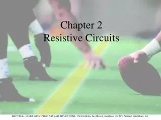
Transpinnor Structure: Isignal Gate Current Gate Insulator B Field B Field Source Ru 15nm Ta 5nm Ferromagnetic CoFeB 3nm Magnetization 6:1 Resistance Change in Tunnel Magnetoresistive (TMR) stack[1] MgO 1.5nm Tunnel Barrier Isignal Ferromagnetic CoFeB 3nm Ru 0.8nm Source CoFe 2nm Antiferromagnetic MnIr 8nm NiFe 5nm Ta 5nm Ru 50nm Ta 5nm Drain Si (001) Substrate Drain Device Area 1μm2 Current Gate [1] Ikeda et. al., Japanese Journal of Applied Physics, Vol. 44, No 48, pp. L1442-L1445
-V Complementary Transpinnor Logic +3mV +V 2.275kΩ or 500Ω 5μA input 5μA output Output Power = 1.6*10-8 W Total Power = 2.5*10-8 W Efficiency=65% 500Ω or 2.275kΩ -3mV
Efficiency for Complementary Transpinnor Circuit 100 90 80 70 60 Efficiency (%) 50 40 Best On/Off ratio today, 4.5:1 30 20 10 0 1 10 100 1000 10000 On/Off Ratio
+ - Transpinnor Logic Example output input A NAND Gate: input B
+ - Transpinnor Logic Example input A NOR Gate: input B output
Transpinnor Structure: Isignal Gate Current Gate Insulator B Field B Field Source Ru 15nm Ta 5nm Ferromagnetic CoFeB 3nm Magnetization 6:1 Resistance Change in Tunnel Magnetoresistive (TMR) stack[1] MgO 1.5nm Tunnel Barrier Isignal Ferromagnetic CoFeB 3nm Ru 0.8nm Source CoFe 2nm Antiferromagnetic MnIr 8nm NiFe 5nm Ta 5nm Ru 50nm Ta 5nm Drain Si (001) Substrate Drain Device Area 1μm2 Current Gate [1] Ikeda et. al., Japanese Journal of Applied Physics, Vol. 44, No 48, pp. L1442-L1445
What is the minimum current required for switching? Isignal Current Gate Insulator 10nm=10-8m B Field B Field Ampere's Law: H = J 2r H = I H needs to be at least H=1 Oersted to switch a GMR device equivalent to B=10-4Tesla (private communication from Stuart Parkin of IBM) (This is equivalent to saying the best relative magnetic permeability is =104 to generate and effective B=1Tesla) I =2r H = 2r (B/o) = 2r 10-4/(4 10-7) and take r=10nm I = 10-8 10-4/(210-7) Amps I = 5 Amps are required for switching! This is really pretty good, but required very optimistic assumptions!
Physics of Wires: l aspect ratio of wire l Repeater Repeater Repeater l RC time = (clock period)/2 a
aspect ratio of wire C = ro a 4800 C 7 femto-Farads <V2> = 4kT R f Vsignal = 0.56 milli-Volts <I2> = 4(kT/R) f Isignal = 0.25 Amps
What is the minimum current required for switching? Isignal Current Gate Insulator 10nm=10-8m B Field B Field I = 5Amps are required for switching! This is really pretty good, but required very optimistic assumptions! According to the previous slide, operation at 1micro-Amp implies a good noise margin ~ 48kT. Operation at 5Amps implies 1200kT per bit function, which is at least 100 better than today's technology, and might be worth pursuing, but it still falls 25 short of the practical engineering limit of 48kT.
That was the Giant Magneto-Resistive Effect. What about the Spin Torque effect? Magnetization is changed by literally transferring the electrons! Take for a minimum domain size, that 1000 electrons have to be transferred. Current I= 1000e- 1.610-19Coul/10-10seconds I=1.610-6Amps = 1.6 Amps Slightly better than the GMR case, but not quite to the theoretical goal<1A. But 1000e- for switching is very optimistic. Further improvements require going slow to keep the current down. Might be interesting at a clock speed <100MHz Source Ru 15nm Ta 5nm Ferromagnetic CoFeB 3nm Ferromagnetic CoFeB 3nm Magnetization Magnetization MgO 1.5nm Tunnel Barrier MgO 1.5nm Tunnel Barrier Ferromagnetic CoFeB 3nm Ferromagnetic CoFeB 3nm Ru 0.8nm Ru 0.8nm CoFe 2nm CoFe 2nm Antiferromagnetic MnIr 8nm Antiferromagnetic MnIr 8nm NiFe 5nm NiFe 5nm Ta 5nm Ta 5nm Ru 50nm Ru 50nm Ta 5nm Ta 5nm Drain Drain Si (001) Substrate Si (001) Substrate
Summary: 1. Giant Magneto-Resistive Effect Switch: Better than today's technology, but not quite to the level of theoretical goal. 2. Spin-Torque Switch: Slightly better than GMR Switch, and capable of achieving theoretical goal at slow clock speeds, <100MHz.
A low-voltage technology, or an impedance matching device, needs to be invented/discovered at the Nano-scale: ~1eV nano-transformer transistor amplifier with steeper sub-threshold slope photo-diode - VG + + + + + MEM's switch Cu solid electrolyte giant magneto-resistance spintronics Cryo-Electronics kT/q~q/C Cu Electro-Chemical Switch
giant magneto-resistance "spintronics" + These switches are made of metallic components and are of inherently low impedance
The other , for energy per bit function 108 107 Gates including wires 106 105 Energy per Bit function (kT) 104 Gates only Technology Gap 103 102 10 1 Transistor Measurements by Robert Chau, Intel 0.1 Shoorideh and Yablonovitch, UCLA 2006 Moore's Law 10μm 1μm Critical Dimension 100nm 10nm 1960 1980 2000 2020 2040 2060 Year
Recommendations: • Milli-Volt powering should be regarded as a Goal for future electronic switching devices. • There would be both an immediate power benefit, as well as a benefit at the end of the roadmap. • Band edge steepness is poorly known, and should be investigated for a number of semiconductors and semi-metals. • The full range of technology options should be included.
Moore You?
! Transistor
Nano-transformers High Impedance Magnetically Loaded Transmission Line
What about very short wires? Johnson Noise: If then the signals could be large enough to be efficiently amplified. The Coulomb Blockade Capacitance. 10 atto-Farads, If For wires less than 1m, a conventional transistor amplifier configuration may be adequate.
The natural voltage range for wired communication is rather low: The natural voltage range for a thermally activated switch like transistors is >>kT/q, eg. ~ 40kT/q or about ~1Volt Voltage Matching Crisis at the nano-scale! If you ignore it the penalty will be (1Volt/1mVolt)2 = 106 The thermally activated device wants at least one electron at ~1Volt. The wire wants 1000 electrons at 1mVolt each. (to fulfill the signal-to-noise requirement >1eV of energy)
In the future, Vdd in digital circuits will drop to 1 milli-Volt, for communication wires.