Dual Switch Flyback Solution
Dual Switch Flyback Solution. Solution for High Efficiency & Low Standby Power to meet 2013 EuP Computing Product Line Power Conversion Taiwan Fairchild Semiconductor. Dual Switch QR Solution . Enabled by FAN6920 : CRM PFC + QR Controller Combo IC FAN7382 : HVIC
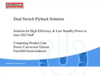

Dual Switch Flyback Solution
E N D
Presentation Transcript
Dual Switch Flyback Solution Solution for High Efficiency & Low Standby Power to meet 2013 EuPComputing Product LinePower Conversion TaiwanFairchild Semiconductor
Dual Switch QR Solution • Enabled by • FAN6920 : CRM PFC + QRController Combo IC • FAN7382 : HVIC • FAN6204 : Syn. Rectifier IC
Basic Operation of Dual Switch Flyback Phase 1: Q1&Q2 On Phase 3&4: Q1&Q2 off, D1&D2 off Phase 2: Q1&Q2 Off, D1, D2 on
Benefit of Dual Switch Flyback (1)Snubber and Leakage Inductance Loss Improved • No snubber loss and heat problem • Leakage inductance is recycled into bulk capacitor Single Flyback iDS iLK Up to 70% of leakage inductance can be recycled Dual Flyback
Benefit of Dual Switch Flyback (2)Low MOSFET Vds and Near ZVS switching • Low MOSFET Drain Source Voltage Good reliability • Allow large n design Near ZVS Switching Low switching loss Vds = Vin + n*Vo + Spike Vds= Vin/2 Spike is clamped by two recycle diodes, stress shared by two MOS Vds of Single Flyback Near ZVS Switching Vds of Dual Flyback Larger switching loss
Benefit of Dual Switch Flyback (3)Low VDS of SR MOS for secondary conduction loss Benefit of high turn ration n to SR MOSFET • VDS of SR MOS is : Vin/n + Vout • Large n Lower VDS Lower MOS Ron in lower price cost & efficiency Example: Vin = 420V, Vo = 12V, n= 12 VDS = 420V/12 + 12V = 47V • Could choose 60V or 75V • SR MOSFET
Benefit of Dual Switch Flyback (4)Built in two level PFC output for low line efficiency • Two Level PFC output to improve low line efficiency When AC > 180V M1 off PFC Vo = 2.5V x (R1+R2)/R2 When AC < 150V M1 on R2//R3 PFC Vo= 2.5V x (R1+R2//R3))/(R2//R3) M1 FAN6920 Block Diagram
Benefit of Dual Switch Flyback (5)Deep extended valley switch for light load efficiency • Deep extended valley switch ( up to 12th valley) to allow low operating frequency in light load Improved light load efficiency Load ↓Freq↑ Poor light load efficiency Freq. nearly constant QR Operation without extended valley switch Other IC: QR Operation with extended valley ( up to 4th valley) 5th valley detect First valley detect 12th valley detect FAN6920 Deep extended valley switch
Benefit of Dual Switch Flyback (6)Power Saving • Dual Switch Flyback Could Meet < 0.5W @ 0.25W ( 2013 EuP) • PFC Stage: • High line/light load Turn off PFC • Low line/light load burst mode • QR Stage: • enter into burst mode when light load • No snubber loss • SR Stage: • Turn off SR when light load
Target Application • For Power Range from 75W ~200W • All in One PC Power • LED TV • Notebook Adapter • Game Console • LED Lighting
Dual Switch Flyback vs. LLC Efficiency: test board 90W/19V No load
Slim Type 19V/ 90W Dual Switch FlybackEfficiency Test Result Efficiency (18 AWG 1.2m wire include): No Load Power Consumption: Input Power @ 0.25W 16.5mm 95mm 60mm
130W/19V AIO power AIO 130W 100mm 145mm Input Power @ no load Input Power @ 0.25W Spec: PIN<0.5W 2013 EUP
200W/19V AIOPower Output Power @ no load Output Power @ 0.25W Output Power @ 0.5W
Follow us on Twitter @ twitter.com/fairchildSemi View product and company videos, listen to podcasts and comment on our blog @ www.fairchildsemi.com/engineeringconnections Visit us on Facebook @ www.facebook.com/FairchildSemiconductor