Download
1 / 50
500 likes | 644 Vues
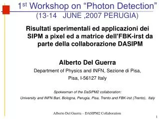
1 st Workshop on “Photon Detection” (13-14 JUNE ,2007 PERUGIA). Risultati sperimentali ed applicazioni dei SIPM a pixel ed a matrice dell’FBK-irst da parte della collaborazione DASIPM Alberto Del Guerra Department of Physics and INFN, Sezione di Pisa, Pisa, I-56127 Italy

E N D
Alberto Del Guerra – DASIPM2 Collaboration 1st Workshop on “Photon Detection” (13-14 JUNE ,2007 PERUGIA) Risultati sperimentali ed applicazioni dei SIPM a pixel ed a matrice dell’FBK-irst da parte della collaborazione DASIPM Alberto Del Guerra Department of Physics and INFN, Sezione di Pisa, Pisa, I-56127 Italy Spokesman of the DaSiPM2 collaboration: University and INFN Bari, Bologna, Perugia, Pisa, Trento and FBK-irst (Trento), Italy
Alberto Del Guerra – DASIPM2 Collaboration SUMMARY • SiPM features • Gain • Noise • PDE • Dynamic Range • Time Resolution • Dependence upon temperature • Radiation Damage • SiPM performance w/Scintillators (i.e., LSO/LYSO) • Energy resolution • Timing resolution • Magnetic field MRI • ASIC • PET Application (FP7 project: COMPANION)
Example: SiPM technology at IRST (TN, Italy) p n+ n+ p epi p+ ≈ ≈ Shallow-Junction GM-APD fully depleted region 4 µm Substrate 500 µm Optimization for the blue light (420nm) 1mm • n+-on-p layer structure • Anti-reflective coating (ARC) optimized for λ~420nm • Very thin (100nm) n+ layer (“low” doping min. recombination) • Thin high-field region (max. doping of p layer also fixes low VBD ) • Trenches for optical insulation of cell (low cross-talk) • Fill factor 20% - 30% (to be optimized) • RQ with doped polysilicon 1mm • SiPM geometry: 1x1mm2 • 25x25 cells • cell size: 40x40 mm2 C.Piemonte NIM A 568 (2006) 224 Alberto Del Guerra – DASIPM2 Collaboration
Dynamic range SiPM output = sum of binary SPAD output ! The output signal is proportional to the number of fired cells as long as the number of photons in a pulse (Nphoton) times the photodetection efficiency PDE is significant smaller than the number of cells Ntotal. Saturation eg: 20% deviation from linearity if 50% of cells respond Best working conditions: Nphoto-electrons < NSiPM cells Alberto Del Guerra – DASIPM2 Collaboration
Time resolution - Experimental Method • SiPM exposed to pulsed femto-second laser • in low light intensity conditions (single photon) • SiPM signal is sampled at high rate and • the time of the pulses measured • by waveform analysis • Time resolution measured by studying • the distribution of time differences between • successive pulses (on the same SiPM device) (G.Collazuol et al. VCI 07) Alberto Del Guerra – DASIPM2 Collaboration
Experimental Setup (CNR Pisa) -Vb Cb Rs hn Vout SiPM gali5 gali5 CC CC CC RL GND LeCroy SDA 6020 Analog bandwidth: 6GHz Sampling rate: 20GS/s Vertical resolution: 8 bits (Aknowledments: E.Marcon, LeCroy) Low noise LV suppliers Crystal for Second Harmonic Generation (SHG) conversion 800 nm400 nm efficiency at % level Pump Laser Millenia V (Spectra-physics) solid state CW visible laser Dark box Ti:sappire laser SiPM + amplifier pump laser SHG External trigger from Ti:sappire laser signal Filters blue + neutral for rejecting IR light and tune intensity Mode-locked Ti:sapphire Laser Tsunami (Spectra-physics) femtosecond pulsed laser wavelength: tuned at 800±15 nm pulse width: ~ 60 fs pulse period: ~ 80MHz pulse timing jitter < 100 fs Electronics I V conversion via RL (500Ω) Two stage voltage amplification (= x50) based on high-bandwidth low-noise RF amplifier: gali-5 (MiniCircuit) Zin= 50Ω (Aknowledments: F.Morsani and L.Zaccarelli, INFN-Pisa) • Data taking conditions: • different Vbias • both at 800 nmand 400 nm • with different light intensities • (counting rates • in the range 10-20 Mhz • ie 15-30 KHz per single cell) Alberto Del Guerra – DASIPM2 Collaboration
Single photon timing resolution FIT: gauss+const Overvoltage=4V λ=400nm Mod (∆t,Tlaser) [ns] FIT: gauss+const +exponential Overvoltage=4V λ=800nm Mod (∆t,Tlaser) [ns] Laser period 1 p.e. ∆t 2 p.e. • Data at λ=800nm • fit gives reasonable χ2 with an • additional exponential term exp(-Δt/t) • Δt ~ 0.2-0.8ns in rough agreement • with diffusion tail lifetime: Δt ~ L2 / p2 D • if L is taken to be the diffusion length • Contribution from the tails ~ 10-30% • of the resolution function area Distributions of the difference in time between successive peaks (modulo the measured laser period Tlaser=12.367ns) Alberto Del Guerra – DASIPM2 Collaboration
IRST – single photon timing • λ= 800 nm • λ= 400 nm e– h+ e– h+ — contribution from noise and method (not subtracted) eye guide high-field region neutral region hν p p+ p n+ depletion region depletion region depletion region Alberto Del Guerra – DASIPM2 Collaboration
CPTA – single photon timing eye guide b) Blue sensitive SSPM 050901B_TO18 a) Green-Red sensitive SSPM 050701GR_TO18 • l = 800 nm •l = 400 nm Two different structures: a) thick n+/p b) p+/n deep junction Alberto Del Guerra – DASIPM2 Collaboration
Comparison with Hamamatsu devices • l = 800 nm •l = 400 nm eye guide HPK-2 HPK-3 1600 cells (25x25) 400 cells (50x50) Alberto Del Guerra – DASIPM2 Collaboration
Dependence of single photon timingon the light spot size and positionBy using pinhole in front of the SiPM • λ=400nm Overvoltage = 4V contribution from noise subtracted — fit to c/√Npe N of simultaneous photo-electrons IRST – timing studies Dependence of SiPM timing on the number of simultaneous photons Poisson statistics: σt∝ 1/√Npe Ø=10mm Ø=25mm Ø=200mm No pinhole Over-voltage = 3V Over-voltage = 5V No relevant spread Uniformity of rise-time among different cells Alberto Del Guerra – DASIPM2 Collaboration
Alberto Del Guerra – DASIPM2 Collaboration Thermal-electrical characterization 1/4 • Ileak vs Bias vs Temperature M. Petasecca et al., Perugia (2007)
Alberto Del Guerra – DASIPM2 Collaboration Thermal-electrical characterization 2/4 • Vbreakdown vs Temperature M. Petasecca et al., Perugia (2007) (**) K.G.McKay,Avalanche Breakdown in Silicon,Physical Review,Vol.94 Number 4, May 1954
Alberto Del Guerra – DASIPM2 Collaboration Thermal-electrical characterization 3/4 M. Petasecca et al., Perugia(2007) • Gain vs Bias vs Temperature The residual Gain dependence is due to the variation of Pt with temperature. …but the Breakdown voltage is dependent with the temperature so…
Alberto Del Guerra – DASIPM2 Collaboration VARIATION with TEMPERATURE Variation of Vbk and Gain with 1 °C ∆T ** J.P.R. David and G.J.Rees, RAD Hard Workshop 2003 * Spanoudaki et al., IEEE NSS-MIC 2005
Radiation damage Expected effects: 1) Increase of dark count rate due to introduction of generation centers • The effect is the same as in normal junction diodes: • independent of the substrate type • dependent on particle type and energy • proportional to fluence Dark rate increase DDC~ Pt/qe• αΦeqVoleff where α ~ 3 x 10-17 A/cm is a typical value of the radiation damage parameter for low E hadrons and Voleff ~ AreaSiPM x GFx Wepi C.Piemonte FNAL 25/10/2006 2) Increase of after-pulse rate due to introduction of trapping centers loss of single cell resolution The few existing preliminary measurements are in agreement with expectations for the radiation damage parameter a within a factor of 2 (Musienko and Danilov, VCI07) Alberto Del Guerra – DASIPM2 Collaboration
Radiation damage Dark count rate increase ~ Positron 28 MeV (8*10**10 cm**2) Photonique/CPTA device Y.Musienko – Vienna VCI 2007 M.Danilov - VCI07 CALICE collaboration MEPhI/Pulsar SiPM Alberto Del Guerra – DASIPM2 Collaboration
Summary of SiPM features • Most important features of a SiPM are: • sensitivity to extremely low photon fluxes • providing proportional information with excellent resolution • and high photon detection efficiency • extremely fast response with low fluctuation (sub-ns risetime and <100ps jitter) • More features: • low bias voltage (<100V) • low power consumption (<50µW/mm2) • long term stability • insensitive to magnetic fields (up to 15T) and EM pickup • robust and compact • low cost (in the future! now ~140$/mm2) + low peripheral costs Technology parameters: may be tuned to match the specific application • silicon quality (dark rate, after-pulse) • doping concentration (operating voltage and its range) • layer structure and thickness (PDE wavelength range, optical cross-talk) • optical cell insulation (optical cross-talk) • effective area of the cells (gain, fill factor, dynamic range, recovery time) • quenching resistor (recovery time, dynamic range) Alberto Del Guerra – DASIPM2 Collaboration
Great variety of possible applications • Calorimetry in magnetic fields • Fiber tracking (spectrometers, beam monitoring) • Particle ID (TOF, RICH, fast timing with cherenkov, Transition Radiation) • Astroparticle (Imaging Air Cherenkov Telescopes) • Space applications (calorimetry, traking, TOF) • Medical imaging (PET) + timing + magnetic and RF fields (MRI) • Thin scintillators read-out • Time resolved X-Ray correlation spectroscopy • Fast timing applications Alberto Del Guerra – DASIPM2 Collaboration
Medical imaging (PET) Many photons applicationBlue sensitive SiPM • Aims: PET detectors with • high spatial resolution (sub-millimeter) • high sensitivity (low dose or high signal/background ratio) • high time resolution (TOFPET background rejection) • DOI capability (no or less parallax) • no sensitivity to magnetic fields, EM pickup and RF (simultaneous NMR scan) • Key issues: • Granularity: matrices of SiPM • High PDE for short wavelengths (420nm): • for coupling to high light yield crystals (scintillators) • max E resolution high efficiency to reject • background Compton scattering • Optical coupling with scintillator • Dynamic range and recovery time: multi cell signal saturation and fluctuation • Gain stability with V and T: individual control of O(10000) channels Alberto Del Guerra – DASIPM2 Collaboration
Matrices of SiPM - IRST The first matrices of 2x2 blue sensitive SiPMs have been developed at IRST G.LLosa et al. IEEE NSS 2006 CD record M06-88 To avoid the anode wire bonding on the active surface aim to use the 3D technology at IRST to have a conducting contact to bring the anode to the backside. SEM photograph of a section of a 3D detector Alberto Del Guerra – DASIPM2 Collaboration
Alberto Del Guerra – DASIPM2 Collaboration SiPMs Scintillator crystals 22Na Source Typical spectrum R ~ 21.0 % FWHM A 22Na spectrum was obtained with a 1 mm x 1 mm x 10 mm LSO crystal coupled to a SiPM (GF~30.9%) Two devices were operated in time coincidence. A typical energy resolution of 21% FWHM was obtained. World best resolution w/ LSO (3x3x20) and PT XP2020 10%(FWHM) [intrinsic 8.9% at 511 keV] [Balcerzyk et al., IEEE TNS 47(2000)1319] Best spectrum R ~ 17.6 % FWHM
Scintillator readout with SiPM matrices • LSO crystal (1x1 mm2) coupled to one pixel - time coincidence with a PMT M6 @ 35.7 R ~ 29%
Scintillator readout with SiPM matrices • LSO crystal (1x1 mm2) put in the centre - time coincidence with a PMT - gain calibration with a LED M6 @ 35.7 R ~ 30%
Timing: set up SiPM LSO CFD thresh1 thresh2 Time coincidence delay trigger scope ∆t
Timing: cosa ci aspettiamo dalla teoria? * Dove… <N> = numero medio di fotoni Q = CFV * <N> = tempo di decadimento dello scintillatore Se… = 40 ns per LSO <N> ~ 100 per il fotopicco Triggerando sul primo fotone Q=1 Triggerando al 20% Q=20 ~ 1.78 ns ~ 400 ps *Post, Schiff Phys. Rev. 80 p.1113 (1950)
Timing: risultati Miglior risultato ottenuto = 600 ps
55 µs SiPM in ststic magnetic field + gradient Magnet 1T Pulse generator LED SiPM Shielded electronics External trigger from gradient amplifier LED trigger scope SiPM signal integrated and histogrammed SiPM signal is acquired while the gradient is increasing
single SiPM in magnetic resonance: Z gradient on Black: reference spectrum acquired inside the magnet with the gradient off Red: spectrum acquired with the gradient on SiPM dark signal Pickup coil signal
single SiPM in magnetic resonance: Z gradient on Black: reference spectrum acquired inside the magnet with the gradient off Red: spectrum acquired with the gradient on LSO (1x1 mm^2) - 22Na - no coincidence R~29.6% Spectra can be superimposed if acquired in a short time R~30.4%
SiPM electrical model Rq: quenching resistor (hundreds of kW) Cd: photodiode capacitance (few tens of fF) Cq: parasitic capacitance in parallel to Rq (smaller than Cd) Cg : parasitic capacitance due to the routing of the bias voltage to the N microcells, realized with a metal grid (few tens of pF) IAV: current source modelling the total charge delivered by a microcell during the avalanche A parameter extraction procedure has been developed, based on both static and dynamic measurements, to perform realistic simulations.
Validation of the parameter extraction procedure Two different amplifiers have been used to read-out the detector b) Voltage amplifier BW=360MHz, Gain=140 a) Transimpedance amplifier BW=80MHz, Gain=2.7kW The fitting between simulations and measurements is quite good
Front-end electronics: main specifications • Self-triggered electronics • Dynamic range: about 50% of SiPM micro-cell occupancy ( SiPM gain 106 , no of micro-cells = 625 total charge 48pC ) • The required jitter for the self-trigger signal (few hundreds of picoseconds) calls for large bandwidth (about 250MHz) • Power consumption: about 2mW per channel • Threshold for the self-trigger signal: adjustable, from few micro-cells to the full dynamic range • Important feature: fine adjustment of the SiPM bias voltage
Front-end architecture Vdd M : 1 To current discriminator SiPM Cf Current buffer VBIAS Rf Vdd Peak detector - Shaper - + + Baseline holder - Vbl + • The front-end is based on an input current buffer, which allows to achieve large bandwidth and dynamic range. • An output branch of the current buffer, suitably scaled, is sent to an integrator, which extracts the charge information. • Another output branch goes to a current discriminator, which provides the self-trigger signal.
The current buffer • A prototype of the input current buffer has been designed, based on a current feedback scheme • Vref can be used to vary the bias voltage of the detector, which is DC coupled to the front-end • The technology used is a standard 0.35mm CMOS • Simulated input impedance 20W • Simulated bandwidth (including the SiPM model connected at the input) 250MHz • Noise negligible • Dynamic range equivalent to about 300 micro-cells
Current buffer: first measurements Output waveform of the test board as a function of the SiPM bias voltage Peak of the output waveform as a function of the SiPM bias voltage • A test board which performs current-to-voltage conversion and amplification has been realized • An infrared pulsed laser has been used as optical source (about 260 micro-cells hit) • The bias voltage of the detector has been varied from 32.5V to 36V • The measurements show the good linearity performance of the current buffer.
Alberto Del Guerra – DASIPM2 Collaboration Proposal COMPANION for FP7 CONFIDENTIAL COMPANION - COmbined MRI-PET for small ANimal-Imaging in Oncology and Neurology • Development of a combined PET/MRI scanner for small animals. • [Submitted 19 April. Results end June. (Start 1 Jan 2008?)] - 8 groups from 4 countries:
Alberto Del Guerra – DASIPM2 Collaboration Design ≤ 2.5 cm 8 cm PET ring 20 cm ~12 cm Split gradient • PET/MRI imposes hard restrictions: • Space limitation inside the MR scanner. • Sensitivity to magnetic fields. • Attempts with light guides and APDs. • Split gradient coil with the PET tomograph placed inside (20 cm outer radius to fit inside standard magnets from 7 to 11T). • PET inner diameter: ~12 cm to accommodate inside RF coils and rat/mouse bed. • Maximum axial length: 8 cm. Maximum transaxial thickness: 2.5 cm.
Alberto Del Guerra – DASIPM2 Collaboration PET design ≤ 2.5 cm ≤ 2.5 cm 2.4 cm 2.4 cm 7.2 cm 12.4 cm 12.4 cm • The PET tomograph consists of a ring composed of 16 detector heads. • The heads are: LSO slab 7.2 cm long x 2.4 cm wide x 1 cm thick; • Read out by SiPM matrices. Total thickness ~1.8 cm.
Alberto Del Guerra – DASIPM2 Collaboration Scintillator SiPM matrix LSO crystal slab: 72 mm x 24 mm 10 mm thick 10 mm 24 mm 72 mm • LSO continuous scintillator slab 7.2 cm x 2.4 cm x 1 cm thick with matrix readout. • Simulations predict better performance than detector heads with pixellated crystals. Better spatial resolution, possible DOI (even with one layer). • Readout by SiPM matrices and dedicated ASIC
Alberto Del Guerra – DASIPM2 Collaboration Matrices • Matrices: Aim- backplane readout • Phase 1: Matrices with lateral readout (1 mm x 1 mm SiPM elements in 1.5 mm x 1.5 mm pitch). • Phase 2: Matrices with backplane readout (1.5 mm x 1.5 mm in 1.5 mm x 1.5 mm pitch -Almost no dead area). • Improved PDE (PET efficiency). • Same layout, number of channels • Development in parallel. Not delaying the PET scanner construction. • Technology already developed at IRST. • Final decision according to performance, yield...
Alberto Del Guerra – DASIPM2 Collaboration Possible layout SIDE VIEW ~1.8 mm scintillator support SiPM matrix ASICs holes to reach the sensor 24 mm … … … cooling pipes TOP VIEW support fan-out … … … 72 mm LATERAL READOUT. BACKPLANE READOUT.
Alberto Del Guerra – DASIPM2 Collaboration Simulation results • Expected performance (GEANT4): • FOV axial 7 cm, transaxial FOV ~6 cm. • spatial resolution at the CFOV , below 1mm3. • efficiency around 11% for an energy threshold of 250 keV. Better than Siemens INVEON
Conclusions • SiPM might really replace PMT in many applications, due to their • sensitivity to extremely low photon fluxes • extremely fast response • IRST developed devices with excellent sensitivity to blue: • devices working as expected • very good reproducibility of the performances • very good yield • very good understanding of the device • flexible geometry (linear and 2-D matrices under development) • Photo-detection efficiency (IRST devices): • Quantum efficiency: > 95% in the blue region (optimized for 420nm) • Triggering probability: growing linearly with overvoltage • Geometrical fill factor: 15-30% to be optimized 44-76% soon available • Single photon timing resolution (IRST devices): • σt at the level of 50ps for typical working overvoltage (4V) • σt at the level of 20ps for ~15 photoelectrons • Applications of SIPM in various fields are under development (e.g. PET) Alberto Del Guerra – DASIPM2 Collaboration
Alberto Del Guerra – DASIPM2 Collaboration Publications by the Collaboration (2006-2007) • F. Corsi, et al.. “Modelling a Silicon Photo Multiplier (SiPM) as a signal source for optimum front-end design”, NIM A, 2007, 572, 416-418. • V.Bindi, et al., “Preliminary Study of Silicon Photomultipliers for Space Missions”, NIM A 2007, 572, 662-667. • N.Dinu, et al., “Development of the first Prototypes of Silicon Photomultipliers (SiPM) at ITC-irst”, NIM A, 2007, 572, 422-426. • C.Piemonte, et al., “Characterization of the first prototypes of Silicon Photomultipliers fabricated at ITC-irst”, IEEE Trans Nucl Sci. 2007, 54(1), 236-244. • C.Piemonte, et al.,“ New results on the characterization of ITC-irst Silicon Photomultipliers”, Conference Records of the 2006 IEEE Nuclear Science Symposium and Medical Imaging Conference, San Diego, USA, October 29-November 4, 2006, cd_ROM, N42-4. • G.Llosa, et al.“Novel Silicon Photomultipliers for PET application” Conference Records of the 2006 IEEE Nuclear Science Symposium and Medical Imaging Conference, San Diego, USA, October 29-November 4, 2006, cd_ROM, M06-88, and submitted to IEEE Trans. Nucl. Sci.(2006). • F.Corsi, et al., “Electrical characterization of Silicon Photo-Multiplier Detectors for Optimal Front-End Design” Conference Records of the 2006 IEEE Nuclear Science Symposium and Medical Imaging Conference, San Diego, USA, October 29-November 4, 2006, cd_ROM, N30-222. • G. Collazuol, et al., “Single timing resolution and detection efficiency of the ITC-irst Silicon Photomultipliers”, presented at the XI VCI, Vienna 19-24 February 2007, accepted for publication in NIM A (2007) • G.Llosa, et al.,”Silicon Photomultipliers for very high resolution small animal PET and PET/MRI”, to be presented at the Second International Conference of the European Society for Molecular Imaging, Napoli, Italy, June 14-15, 2007 (Abstract) • G.Llosa et al. “ Novel Solid State detector and their application to very-high resolution PET and Hybrid Systems.” to be presented at the ENC 2007, Brussels, 16-19 September 2007, and submitted to Radiation Protection Dosimetry • A. Del Guerra “Silicon photomultiplier(SIPM): the Ideal Photodetector for the Next Generation of TOF, DOI, MRI compatible, High Resolution, High Sensitivity PET”, to be presented at the “Joint Molecular Imaging Conference” , Sept 8-11, 2007, Rhode Island, NY(USA) • + 1 submission to X EFOMP (sept 2007) • + 4 submissions to IEEE NSS MIC 2007 (nov 2007)
Alberto Del Guerra – DASIPM2 Collaboration International grants and collaborations (Pisa based) Established • Marie Curie Individual Fellowship (2007-2008) • Italy-UK [Pisa-Cambridge (2007)] • Italy-Spain [Pisa-Valencia (2007-2008)] • Pisa University- UCI (US) Requested • NIH (US) (2nd revision) {P.I. w/ Univ. of Washington} • FP7 • COMPANION {P.I. w/ other seven partners} • PEM-MRI {partner}
Alberto Del Guerra – DASIPM2 Collaboration Acknowledgments Deepest thanks go to the members of the DASIPM2 collaboration: • Claudio Piemonte & collaborators (FBK-irst and Trento) • Francesco Corsi & collaborators (Bari) • Giovanni Ambrosi & collaborators (Perugia) • Giuseppe Levi & collaborators (Bologna) • Pisa TEAM (Gabriela Llosa, Sara Marcatili, Gianmaria Collazuol, S. Moehrs, N.Belcari, Maria G. Bisogni)
Alberto Del Guerra – DASIPM2 Collaboration THE END THANK you!