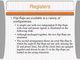
Registers
Registers. D Q. D Q. D Q. D Q. D Q. 4. 4. A 4-Bit Register. D3. Q3. CLK. D2. Q2. D. Q. CLK. CLK. D1. Q1. Could be called a parallel-in/parallel-out register. Why?. CLK. D0. Q0. CLK. D Q. D Q. D Q. D Q. A Shift Register. Q3. Q2. Q1. Q0. SerIn.

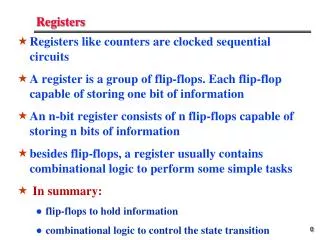
Registers
E N D
Presentation Transcript
Registers ECEn 224
D Q D Q D Q D Q D Q 4 4 A 4-Bit Register D3 Q3 CLK D2 Q2 D Q CLK CLK D1 Q1 Could be called a parallel-in/parallel-outregister. Why? CLK D0 Q0 CLK ECEn 224
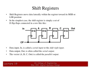
D Q D Q D Q D Q A Shift Register Q3 Q2 Q1 Q0 SerIn CLK CLK CLK CLK Called a serial-in, parallel-out shift register (SIPO) ECEn 224
D Q D Q D Q D Q SIPO Register (Serial-In/Parallel-Out) Parallel-Out Q3 Q2 Q1 Q0 SerIn CLK CLK CLK CLK ECEn 224
D Q D Q D Q D Q SISO Register (Serial-In/Serial-Out) SerOut SerIn CLK CLK CLK CLK Useful for delaying a serial bit-stream some number of cycles… ECEn 224
D Q D Q 4 4 4 4 How to Make Any of These Loadable? D Q D Q CLK CLK LOAD This register loads on everyclock cycle. How to make it load when told to? An obvious solution… This is incorrect – why? ECEn 224
D Q LOAD CLK D Q Gated Clocking Is A Bad Thing To Do… GatedClock tAND The flip flopgets its clocksignal late Thus, itsoutput appears late… CLK LOAD GatedClock ECEn 224
Gated Clocking • Causes different flip flops to load at different times • A form of clock skew • Makes doing timing analysis more difficult • Can lead to circuits which run more slowly • Can lead to circuits which fail at any clock rate ECEn 224
D Q D Q QA Q FFA FFB LOAD GatedClock CLK CLK Value that should be loaded into FFB (‘1’) tCLK-Q tAND Value that gets loaded into FFB (‘0’) CLK QA LOAD GatedClock ECEn 224
D Q D Q QA Q FFA FFB If tCLK-Q < tAND: FFB loads wrong value LOAD GatedClock CLK CLK Value that should be loaded into FFB (‘1’) tCLK-Q tAND Value that gets loaded into FFB (‘0’) CLK QA LOAD GatedClock ECEn 224
Globally Synchronous Design • One global clock • All registers load on that clock’s edge • Control over loading done via input forming logic (IFL) • Simplifies timing analysis and requirements • Makes it possible for even novices to design large, functioning circuits • Multi-clock circuits next semester’s topic ECEn 224
D Q 0 1 The Correct Way To Make A Loadable Register (1-Bit) Q DIN LOAD CLK When LOAD=0, FF loads old value When LOAD=1, FF loads DIN ECEn 224
D Q D Q 0 1 A Correct Scenario Q QA FFB FFA LOAD CLK CLK No clock skew Both FF’s load on exactly same clock edge Both Q’s appear at same time Timing analysis greatly simplified ECEn 224
D Q 4 4 4 4 0 1 A Loadable Parallel-In, Parallel-Out Register Q(3:0) DIN(3:0) LOAD CLK PIPO ? ECEn 224
D Q D Q D Q 0 1 0 1 0 1 A Loadable Parallel-In, Serial-Out Register (PISO) SerIn SerOut LOAD/SHIFT# CLK LOAD/SHIFT# CLK LOAD/SHIFT# CLK D2 D1 D0 When LOAD/SHIFT# = 1, register loads D2…D0 When LOAD/SHIFT# = 0, register shifts right This register is always either loading or shifting ECEn 224
MUX for Register Control • Loadable register concept can be generalized to provide any combination of inputs to register • Load, clear, set, enable, left shift, right shift, increment, etc. ECEn 224
D Q D Q D Q 0 1 0 1 0 1 A SISO With An Enable Input SerOut SerIn ENABLE ENABLE ENABLE CLK CLK CLK Combination of loadable register with shift register… When ENABLE=0, register doesn’t shift (re-loads old value) When ENABLE=1, register shifts ECEn 224
D Q D Q D Q 0 1 0 1 0 1 Q1 Q0 Q2 UP/DOWN# UP/DOWN# UP/DOWN# CLK CLK CLK A Bidirectional Shift Register TopIn Q1 Q2 Q0 Q1 BottomIn ECEn 224
Uses of Shift Registers • Collecting serial input data into a parallel word • Shifting out bits of a word • Delaying a serial stream by some # of cycles ECEn 224
D Q 4 4 4 4 4 4 A Clearable Counter Q Q+1 Q 0 Q 2 CLK CLR INC From there to here, from here to there, interesting circuits are everywhere… (when you have a MUX and some flip flops) ECEn 224
D Q 4 4 0 1 An Up/Down Counter Q-1 Q Q+1 CLK UP/DN# How about an up/down counter + bi-directional shift register design? ECEn 224
D Q 4 4 4 4 4 4 Up/Down Counter + Bi-Directional Shift Register Q+1 Q-1 Q Q<<1 Q>>1 2 CLK Control ECEn 224
D Q D Q 4 4 4 4 4 4 0 1 0 1 An Accumulator • Values to be added are placed on A input, one per cycle. Register accumulates their sum. Version A Version B + + A A Q Q 0 CLR LOAD CLK CLK This one loads 0 when CLR=1 This one loads A when LOAD=1 Both work, they just have different timings… ECEn 224
Register Files Small memories holding multiple words of data ECEn 224
Typical Register File DataIn n clk regWE RegFile Addr m n DataOut ECEn 224
Data to be written toregister file Typical Register File DataIn n clk regWE RegFile Addr m n DataOut ECEn 224
Data to be written toregister file Data that is read fromregister file Typical Register File DataIn n clk regWE RegFile Addr m n DataOut ECEn 224
Data to be written toregister file Address that readsand writes are for Data that is read fromregister file Typical Register File DataIn n clk regWE RegFile Addr m n DataOut ECEn 224
Data to be written toregister file Address that readsand writes are for Data that is read fromregister file Typical Register File DataIn n clk regWE This register will hold2m words, each n bitswide RegFile Addr m n DataOut ECEn 224
Data to be written toregister file Controls whetherreading or writing Address that readsand writes are for Data that is read fromregister file Typical Register File DataIn n clk regWE This register will hold2m words, each n bitswide RegFile Addr m n DataOut ECEn 224
Reads are asynchronous(combinational) Writes occur on the clock edge. Data to be written toregister file Controls whetherreading or writing Address that readsand writes are for n Data that is read fromregister file Typical Register File DataIn n clk regWE This register will hold2m words, each n bitswide RegFile Addr m DataOut ECEn 224
n n n n n n n n n n Building a Register File Reg0 Write Decoder Reg1 Reg2 Reg3 Register write signals 8:1 MUX DataOut Reg4 Reg5 Reg6 Reg7 m=3 regWE DataIn clk Addr ECEn 224
Asynchronous read:just a MUX n n n n n n n n n n Building a Register File Reg0 Write Decoder Reg1 Reg2 Reg3 Register write signals 8:1 MUX DataOut Reg4 Reg5 Reg6 Reg7 m=3 regWE DataIn clk Addr ECEn 224
Loadable registers Asynchronous read:just a MUX n n n n n n n n n n Building a Register File Reg0 Write Decoder Reg1 Reg2 Reg3 Register write signals 8:1 MUX DataOut Reg4 Reg5 Reg6 Reg7 m=3 regWE DataIn clk Addr ECEn 224
Loadable registers Asynchronous read:just a MUX 3:8 Decoderwith enable n n n n n n n n n n Building a Register File Reg0 Write Decoder Reg1 Reg2 Reg3 Register write signals 8:1 MUX DataOut Reg4 Reg5 Reg6 Reg7 m=3 regWE DataIn clk Addr ECEn 224
Regk Reg0 Qk regWEk Load Q Reg1 D Reg2 clk Reg3 Register write signals DataIn Reg4 n n n n n n n n n Reg5 Reg6 Reg7 n n DataIn clk Loadable Register ECEn 224
3:8 Decoder Write Decoder Register write signals Register write signals m=3 regWE Addr m=3 regWE Addr Write Decoder ECEn 224
Multi-Ported Register File Reg0 Write Decoder One write port, oneread port.Different write andread addresses Can be reading fromone location on samecycle you write to another location Reg1 Reg2 Reg3 DataOut Register write signals 8:1 MUX Reg4 Reg5 Reg6 Reg7 RAddr WAddr WE DataIn clk ECEn 224
Multi-Ported Register File Reg0 Write Decoder One write port Two read ports Can be reading fromtwo locations on samecycle you write to another location Useful for microprocessor design Reg1 Reg2 Reg3 DataOut1 Register write signals 8:1 MUX Reg4 Reg5 DataOut2 Reg6 Reg7 WAddr WE DataIn clk Raddr2 RAddr1 ECEn 224
Memories vs. Register Files • Random Access Memory (RAM) is similar to a register file • Stores many multi-bit words for reading/writing • RAM usually only single-ported • RAM usually much, much larger • Mbytes instead of bytes • RAM implementation conceptually the same as register file • Transistor-level implementation different due to size/usage characteristics • RAM design beyond the scope of this class ECEn 224