Download
1 / 10
100 likes | 222 Vues
Over a decade of research has highlighted the need for innovative techniques in ultrafast science. The combination of soft X-ray magnetic holography and electron microscopy enables deeper understanding and control of material processes at the nanoscale. As we aim to unlock the mysteries of ultrafast and ultrasmall phenomena, integrating both X-ray and electron-based methods will provide unprecedented insights into atomic-scale dynamics. Key challenges include developing user facilities and novel mechanisms to probe electron and spin behaviors, paving the way for revolutionary advancements in materials science.

E N D
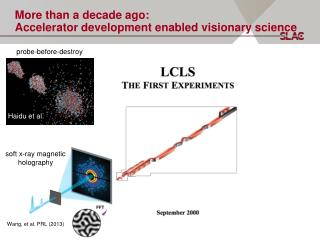
More than a decade ago: • Accelerator development enabled visionary science • probe-before-destroy • Haidu et al. • soft x-ray magnetic holography • Wang, et al. PRL (2013)
Today: We need the complementarity of x-rays & electrons • to access to the “Ultrafast” & “Ultrasmall” • FePt • heat sink • 2nm • Goal: understand & control materials processes • probes electrons & spins • probes lattice • G. Bertero (WD Corp.) • soft x-ray magnetic holography • nano-UED • Xiang, et al. SLAC report (2014) • Wang, et al. PRL (2013)
X-rays or electrons? We need both! • Electrons: • can be manipulated by electric & magnetic fields (microscopy) but have <10nm coherence lengths. • X-rays: • Fully coherent beams offer new opportunities for holographic imaging. Soft x-ray resonant inelastic cross sections are comparable to those of electrons, elastic cross sections are much lower. • R.Henderson,Quarterly Reviews of Biophysics 28 (1995) 171-193.
The Future of Electron Scattering & Diffraction • Opportunities for Ultrafast Science • Key Breakthrough Science Opportunities and Challenges • Atomic Scale Molecular Processes • Photonic Control of Quantum Materials • Energy Transport at the Nanoscale • Mesoscale Materials and Phenomena • Evolving Interfaces, Nucleation, and Mass Transport • DOE Basic Energy Sciences Needs Workshop Report (2014)
The Future of Electron Scattering & Diffraction • How do we get there? • UEM • User Facility • Nano-UED • User Facility • Ultrafast • Electron • Microscopy • Ultrafast • Electron Diffraction • DOE Basic Energy Sciences Needs Workshop Report (2014)
Controlling processes on the level of electrons: • Non-Born-Oppenheimer dynamics in molecules • requires sub-100 fs with unfocused electron beam at high repetition rates • (UED) • Ben-Nun and Martinez, Chem. Phys. 259, 237(2000) • Absorption triggers coupled ultrafast motion of nuclei and electrons, hard to model • Born-Oppenheimer violation provides fast funnels for steering energy into particular channel • M. Centurion Lab • U. Nebraska • Aligned CF3I • Guehr, et al.
Opportunities for Ultrafast Materials Science • nanoscale energy transport • requires sub-100 fs with focused electron beam at high repetition rates • (nano-UED) • nanoscale mechanisms of phase transitions • photonic control of quantum materials
Imaging of Nanoscale Processes • Phase transitions: diffusionless vs. mass transport • requires single-shot imaging • (10ps - 10 nm UEM) • Biological processes • Carbon fixation by bacterial carboxysomes
Early Science Opportunities with UED • Gas phase chemistry (sub-100fs & 100μm beam size): Experimental setup is still under development (requires isolation of gun and sample vacuum). • UEM • User Facility • Materials science will initially be limited by available samples: • etching, exfoliation, sample growth of ~ 100μm free standing films needs to be developed) • Nano-UED • User Facility • Ultrafast • Electron • Microscopy • Development of laser-electron cross correlation schemes: • use laser-induced space charge • electron beam induced dynamics • photo-induced electron-lattice coupling in wide-bandgap oxides • Ultrafast • Electron Diffraction
Early Science Opportunities with UED • Gas phase chemistry (sub-100fs & 100μm beam size): Experimental setup is still under development (requires isolation of gun and sample vacuum). • First results (A. Reid, R. Li, P. Musumeci) • Materials science will initially be limited by available samples: • etching, exfoliation, sample growth of ~ 100μm free standing films needs to be developed) • Development of laser-electron cross correlation schemes: • use laser-induced space charge • electron beam induced dynamics • photo-induced electron-lattice coupling in wide-bandgap oxides • Measurement of single-shot electron diffraction from a 40nm FeRh film epitaxially grown on 10 nm MgO IBAD deposited on 100nm SiN.