Download
1 / 27
280 likes | 518 Vues
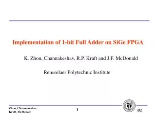
Implementation of 1-bit Full Adder on SiGe FPGA. K. Zhou, Channakeshav, R.P. Kraft and J.F. McDonald. Rensselaer Polytechnic Institute. 1. Outline. Introduction to FPGA architecture Short overview of IBM SiGe HBT BiCMOS Technology (5HP, 7HP and 8NT)

E N D
Implementation of 1-bit Full Adder on SiGe FPGA K. Zhou, Channakeshav, R.P. Kraft and J.F. McDonald Rensselaer Polytechnic Institute 1
Outline • Introduction to FPGA architecture • Short overview of IBM SiGe HBT BiCMOS Technology (5HP, 7HP and 8NT) • Conventional Xilinx 6200 design • Redesigned CLB architecture • SiGe FPGA architecture description • Test Circuits • Performance • Conclusion • Future plan 2
FPGA Introduction I/O Cell Basic Cell Vcc Configuration data Vee Configuration Memory planes 3
SiGe Technology Eg,Ge(grade) = Eg,Ge(x=Wb) - Eg,Ge(x=0) • A small quantity of Germanium (Ge) is added to the base of the BJT. • There exists a drift field in the base, which aids the faster movement of minority carriers. This reduces the base transit time and hence increases the cutoff frequency. • The Ge mole fraction varies from 3~9% in the base region. (From J.Cressler, “SiGe HBT Technology: A new Contender for Si-Based RF and Microwave Circuit Applications”, IEEE Transactions on Microwave Theory and Techniques, Vol. 46, No. 5, May 1998, 572-589.) 4
Performance Issues of SiGe Devices • Bandgap Engineering + Conventional Si fabrication technologies • Co-integrated with CMOS process: very low initial investment • SiGe HBT + Si CMOS = SiGe BiCMOS • Higher current gain ( SiGe ) • Higher cutoff frequency ( fT ) • Higher early voltage (VA) • Advantages over III-V materials • GaAs or InP have no decent grown oxide • III-V wafers are smaller with higher defect densities Lower cost SiGe will replace GaAs in many high frequency applications 5
SiGe RFIC Markets GPS (Global Positioning System), CNS (Car Navigation System), B-WLL (Broadband Wireless Local Loop) ITS (Intelligent Transportation System), DSRC (Dedicated Short Range Communication) (From http://www.flash-comm.com/products/market/market_over.pdf) 6
What is Current Mode Logic? Vcc 0 V Fastest Logic Level Limited Drive Capability Level 1 -250 mV -950 mV Inter-block Signal Level Good Fan-Out (10) Level 2 -1.2 V -1.90 V Clock Signal Slowest Level Level 3 -2.15 V (VBE is approximately 0.703 V when Ie is 10 A) Vee -3.4 V 7
Programmable Bipolar Logic • 1983: Fairchild ECL Field Programmable Logic Array • Fuse Based • 4ns Cycle Rate • High Power • Scaling Problems • 1990: Algotronix 1.2uM 256 Cell Configurable Logic Array • fT -6 GHz, 200ps Gate Delay • 4 Transistor Static RAM Memory Cells • ASIC Emulation and Signal Processing • Forerunner of XC6200 (C. Carruthers, T. Kean, “Bipolar CAL chip doubles speed of FPGAs”, Oxford 1991 International Workshop on Field Programmable Logic and Applications, 1991, pp.46-53.) 9
CLK S Clr S4 N S E W N4 S4 E4 W4 Nout E4 E X3 N E W F N S E W N4 S4 E4 W4 N S E W N4 S4 E4 W4 X2 X1 CLB F N S E F N S W F Eout Wout X2 X3 S E W F W W4 MAGIC Sout Clk N4 N CLR Xilinx 6200 Architecture Logic Cell || CLB + Routing Multiplexers • 4output multiplexers • 3 input multiplexers • 1 magic multiplexer 10
A AND B (X1=A X2=B X3=A) Input Multiplexers X1 If A=1 then select Y2 output = B If A=0 then select Y3 output = 0 X2 Y2 1 CS Multiplexer 0 RP Multiplexer C F S DQ X3 A OR B (X1=A X2=A X3=B) Y3 Clk Q If A=1 then select Y2 output = 1 If A=0 then select Y3 output = B Clr Configurable Logic Block (CLB) Architecture 11
Objective of the New Architecture • Decrease the propagation delay. • Use fewer trees. • Reduce the power consumption. • Design the FPGA based on multiplexers, not pass transistors, the bottleneck of the CMOS FPGA. • Design the high speed part with Bipolar and the low speed part with CMOS. 12
Redesigned CLB Architecture A B C D X1 X2 Y2 a a 1 0 RP Multiplexer C F c S DQ DQ OUT X3 Y3 CS Multiplexer Clk Clk Q Q Clr b Slave latch Block3 Master latch To 9:1 Muxes Block1 Block2 13
VCC 0 V OUT OUT X2 X2 X2 X2 X2 X2 X2 X2 X3 X3 X3 X3 X3 X3 X3 X3 X1 X1 X1 X1 X1 X1 X1 X1 D A B C Vee -2.8V CLB Block Circuits • Two level CML multiplexer • Control logic is not differential Block1 14
CLB Block Circuits (cont.) V V 0 V 0 V CC CC OUT OUT OUT OUT a a a a Diode is used here to preventbreakdown b b b b Clk Clk Clk Clk E E F E Block2 V V - - 2.8V 2.8V ee ee 15
V V 0 V 0 V CC CC c c a a a a c c OUT OUT OUT OUT Clk Clk Clk Clk E Clr Clr E Block3 V V - - 2.8V 2.8V ee ee CLB Block Circuits (cont.) Emitter follower is used to drive the output multiplexers 16
CLK Nout S Clr S4 S W Q N N4 E S4 E4 W4 E4 Vcc Configuration data E 2:1 Multiplexer N E W F X3 N N S S X2 X1 E E W W CLB MUX N4 N4 S4 S4 E4 E4 W4 W4 Q Q F N N Eout Wout S S CLB Configuration Bits E E Vee F F W X2 X3 N S E F W4 MAGIC Two Configuration Memory planes Sout Clk N4 N CLR Configuration Memory 17
CLB Configuration CLB configuration as a 2:1 Mux 18
CLB Configuration (cont.) CLB configuration as an XOR gate 19
1-bit Full Adder with waveforms schematics Propagation delay is 214ps 20
CLB Performance • Note: • The simulation is done under 25 ºC and with no load. The propagation delay of CLB is 48 ps under normal loads. • The combinational path and the sequential path can not be on simultaneously. • The power supply is 2.8 V. 21
FPGA Performance • Note: • Typical loading values are used. • Delays vary depending on direction. Only maximum delays are listed here. • XC6200 operates at –2 speed grade (maximum speed). 22
CLB CLB Cell CLB CLB Cell Test Circuits Goal: To test the propagation delay of the logic cell Goal: To test the propagation delay of the CLB 23
Layout of the Test Circuits CLB ring FPGA ring 24
Progress made SiGe reticle Testing Probes Our first chip 25
Conclusion • SiGe is an obvious solution to offer both speed and easy processing. • The long turn around time faced by high-speed circuits can now • be reduced by using SiGe FPGAs for prototyping. • The new FPGA design effectively combines high speed SiGe with • low power CMOS. Hence, it has a better performance in terms of • power and speed. • The number of global lines have been reduced by the new decoding • scheme. 26
Future Plan • Reduce the number of trees in the FPGA. • Complete the “selective tree shutdown” idea. • Testing and characterization of fabricated chips this summer will direct future designs. • With the recent availability of 7HP (8NT is expected shortly), the FPGA can run at over 10 GHz. The chip has already been submitted to IBM and is supposed to be back in September. • Above 10 GHz, transmission line effects require shortening long wires (a few hundreds of microns). 27