Download
1 / 22
721 likes | 4.57k Vues
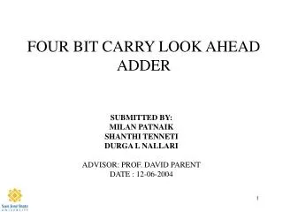
4-bit Carry Look Ahead Adder. Samira Sharma Suneera Sharma Advisor: Dave Parent 12/6/04. Agenda. Abstract Introduction Why Simple Theory Summary of Results Project (Experimental) Details Results Cost Analysis Conclusions. Abstract.

E N D
4-bit Carry Look Ahead Adder Samira Sharma Suneera Sharma Advisor: Dave Parent 12/6/04
Agenda • Abstract • Introduction • Why • Simple Theory • Summary of Results • Project (Experimental) Details • Results • Cost Analysis • Conclusions
Abstract • We designed an 4-bit carry look ahead adder that operated at 200 MHz and used 16mW of Power and occupied an area of 420x440mm2
Introduction • Why is a Carry Look Ahead Adder important? • The CLA is used in most ALU designs • It is faster compared to ripple carry logic adders or full adders especially when adding a large number of bits. • The Carry Look Ahead Adder is able to generate carries before the sum is produced using the propage and generate logic to make addition much faster.
Equations for Logic of 4-bit CLA Gi = Ai.Bi Pi = (AiÅ Bi) C1 = G0 + P0.C0C2 = G1 + P1.C1 = G1 + P1.G0 + P1.P0.C0C3 = G2 + P2.G1 + P2.P1.G0 + P2.P1.P0.C0C4 = G3 + P3.G2 + P3.P2.G1 + P3P2.P1.G0 + P3P2.P1.P0.C0 Si = AiÅ BiÅ Ci = PiÅ Ci.
Project Summary • We used the gate design methodology instead the AOI design method for Carry logic because of its lesser drain caps we were able to meet timing specifications, also, made hand calculations easier to do. • We used a less complicated design and created separate cells in order make debugging easier and also allow for a neater layout.
Design Flow Functions and Specs Designing For Logic Hand Calculations Initial Sizing Stick Diagrams Layout DRC & Extraction LVS Post Extraction
Longest Path Calculations tPHL = 5ns/11 = 0.45ns Note: All widths are in microns and capacitances in fF
Final Simulation Test Vectors A=1 B=0 Cin= 1111 +0000 1111 1 1111 0000 10000
LVS Verification Net-lists match!
Cost Analysis • verifying logic = 10 hours • verifying timing = 20 hours • Layout = 50 hours • post extracted timing = 5 hours
Lessons Learned • Learn the tradeoffs of AOI vs. Gate Design Methodology -Area Constraints -Timing Constraints • Develop Good testing and debugging skills. • Have Fun!
Summary • We met specifications by designing a 4-bit Carry Look Ahead Adder -Rise time= Fall time= 2.65 ns -Total Area= 420x440mm2 -Power= 16 mW • In the future this circuit design can be designed using less power and operating at a higher frequency.
Acknowledgements • Thanks to Cadence Design Systems for the VLSI lab • Thanks to all our classmates that helped us in the lab • Professor David Parent for setting us up for success! • Undo, Stretch, Copy, Move and Metal 1,2 and 3!