Download
1 / 15
160 likes | 829 Vues
4 Bit ALU with Carry Look Ahead Generator. Piyu Singh Dhaker Kedar Bhatawadekar Nikhat Baig Advisor: Dave Parent DATE:12/05/05. Agenda. Abstract Introduction Project Details Circuit Diagram and Longest path calculation. Project Schematic and Experimental Details Lessons Learned

E N D
4 Bit ALU with Carry Look Ahead Generator Piyu Singh Dhaker Kedar Bhatawadekar Nikhat Baig Advisor: Dave Parent DATE:12/05/05
Agenda • Abstract • Introduction • Project Details • Circuit Diagram and Longest path calculation. • Project Schematic and Experimental Details • Lessons Learned • Conclusions
Abstract • Referred product specifications of Philips Semiconductor 74HC/HCT181 (4-bit ALU). • Successfully Designed a 4-bit ALU using cadence CAD tools with AMI06(0.6um) process specification.The design has successfully passed DRC and LVS and meets the clock frequency of 250MHz consuming 19.5mW power and area 360x400um2
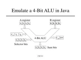
Introduction • Arithmetic and Logic Unit is the heart of a microprocessor and is embedded in almost every digital system that manipulate numbers. • Look-ahead carry is capable of preprocessing the two numbers being added to determine the carry ahead of time decreasing delay.
Project Details • A full carry look-ahead scheme was implemented for fast, simultaneous carry generation by means of two cascade outputs G and P for the four bits in the package. • High-speed arithmetic operations can be performed. • These logic functions are selected using the four function select inputs (S0, S1, S2, S3) with mode-control input (M) at logic high level to disable the internal carry.
Longest Path Calculations f=250 MHz T=4ns No of logic levels:13 tphl= T/(13+4)------------------------------for each stage =2.35E-10 s
Design Flow • Test the entire schematic with NC Verilog for logic verification • After longest path calculation start with the schematic and layout of components in longest path. • Assemble individual components into AOIs. • Assemble AOIs to form the entire schematic • Add DFFs at the input.
Lessons Learned • Use the Hierarchical Design Approach. • Proceed to the next stage only after DRC and LVS succeed and Extracted meets the specifications • No routing in Poly and all cells same height. • Starting early and proper organization of tasks help to meet project deadlines.
Acknowledgements • We thank Dr. Parent for being easily approachable with flexible timing and replying promptly to every query we came across. • We thank M/s Cadence Design Systems for the VLSI Lab. • We thank M/s Synopsys for Software donation. • Our sincere thanks to every person that shared their knowledge with us which helped us in our quest to achieve strong performance in project.