Download
1 / 22
250 likes | 496 Vues
Design of 4-bit ALU. Revati Ingale Madhuri Kakulavarapu Advisor: David W. Parent 17 th May 2004. Agenda. Abstract Introduction Why Simple Theory Back Ground information (Lit Review) Summary of Results Project (Experimental) Details Results Cost Analysis Conclusions. Abstract.

E N D
Design of 4-bit ALU Revati Ingale Madhuri Kakulavarapu Advisor: David W. Parent 17th May 2004
Agenda • Abstract • Introduction • Why • Simple Theory • Back Ground information (Lit Review) • Summary of Results • Project (Experimental) Details • Results • Cost Analysis • Conclusions
Abstract • Goal is to design a 4-bit ALU driving up to 30fF. • Arithmetic operations are A+B, A+B+1, A+ B`, A– B, Transfer A, Transfer B, A + 1, B -1. • Logical operations are A Ex-OR B, A AND B, A OR B, NOT A. • The data should be transferred at clock rates of 200 MHz , with 1ns setup and hold times. • Maximum power is 100mW. • Maximum area is 500×500 µm2
Introduction Why this project? ALU is a building block of several circuits. • Challenging to design a 16 logic level design working at 5ns. • Challenging to layout. • Design consists of different kinds of logic… Look Ahead Carry Generator logic, Full adder, Subtractor, Transfer Data, DFF, Super Buffer, MUX, Transmission gate, Decoders, Inv, Nand, Nor, Ex-Or, etc.
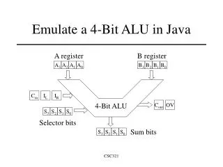
Function Table A, B = 4 Bit Input, X = don’t care Condition M , S0, S1 = Status Control Pin Cin = Carry in; Cout = Carry Out
Block Diagram Super Buffer Carry Generator Subtractor & Transfer Decoder Adder Arithmetic Unit Bank of 9 DFFs Bank of 5 DFFs T-gate Based MUX XOR AND OR INV MUX-2 Logical Unit
Project Summary • The Look Ahead Carry logic makes the Arithmetic unit much faster than the conventional Ripple Carry adder. • The ALU performs Eight Arithmetic functions and Four Logical functions at 200MHz.
Logic Level Gate Cg to Drive #CDNs #CDPs #LNs #LPs Wn Wp Cg of gate 1 XOR2 30 3 3 2 2 4.05 6.45 17.8 2 INV 17.8 1 1 1 1 3.15 4.65 13.1 3 NOR2 13.1 2 3 1 2 2.1 6.3 14.4 4 NAND2 14.4 3 2 2 1 2.55 2.85 9.1 5 INV 9.1 1 1 1 1 3.15 4.65 13.1 6 NOR2 13.1 2 3 1 2 2.1 6.3 14.4 7 NAND3 40 5 3 3 1 9.6 8.4 30 8 INV 50 1 1 1 1 6.75 10.35 25 9 INV 25 1 1 1 1 2.25 3.45 9.7 10 XOR2 40 3 3 2 2 4.05 4.05 17.8 11 NAND2 40 3 2 2 1 4.5 4.95 16 12 XOR2 20 3 3 2 2 4.05 6.45 17.8 13 INV 17.8 1 1 1 1 2.25 3.45 9.7 14 NAND3 9.7 5 3 3 1 2.4 2.1 7.6 15 INV 40 1 1 1 1 4.5 6.75 1.5 Longest Path Calculation (Arith. Unit) Note: All widths are in microns and capacitances in fF. Time Delay at complex gate like XOR is bit more than delay at INV etc.
D Flip Flop Decoder
Look Ahead Carry Generator 2 Select Pin Mux
T gate for Mux Super Buffer
Simulation-1(Arith.Unit) M, S1, S0, Cin are set for A-B operation and A3, A2, A1, A0 are set to 1111.
Simulation –2 (Logical Unit) M, S1,S0 are set for XOR operation and A3,A2,A1,A0 are set to 0110.
Results • The ALU performs all 12 functions at a 200Mhz clock and a load of 30fF. • Worst-case Power dissipation is 26.7 mW. • Area of the layout is 530×515µm2.
Cost Analysis • Time spent on each phase of the project • Logic design 1 week. • Logic check 1 week. • Gate level design 1 week. • Integration of schematic blocks 2 weeks. • Timing check 2 weeks. • Layout 3 weeks. • Post extraction check 3 days.
Summary • Designed and tested almost all the design units that we learnt in the class. • Designed a 4-Bit ALU that performs eight arithmetic and four logical functions at 200MHz frequency with setup and hold time 1ns, driving up to 30fF. • This circuit can be used as a building block for 16/32-bit ALU. • The Logic design can be modified to perform more functions.
Acknowledgements • Thanks to Cadence Design Systems for the VLSI lab • Thanks to Professor David W. Parent for his guidance.