4-bit ALU
4-bit ALU . Cailan Shen Ting-Lu Yang Advisor: Dr. Parent May 11, 2005. Agenda. Introduction Project (Experimental) Details ALU design in Cadence DFF, MUX and Adder Summary Project result Lesson learned. Introduction.


4-bit ALU
E N D
Presentation Transcript
4-bit ALU Cailan Shen Ting-Lu Yang Advisor: Dr. Parent May 11, 2005
Agenda • Introduction • Project (Experimental) Details • ALU design in Cadence • DFF, MUX and Adder • Summary • Project result • Lesson learned
Introduction • The 4-bit ALU that our group designed can perform following functions: • Add, Subtract, NOR, OR, and AND. • The 4-bit ALU operates at 200 MHz with an area of 300 um x 320 um and use 1.3 mW power. • The 4-bit ALU is made up of 4 identical 1-bit ALU, and DFFs ensure the 4-bit ALU to obtain the correct inputs and send out correct outputs. • This project is worthwhile because this ALU has all the logic blocks that we learned in class.
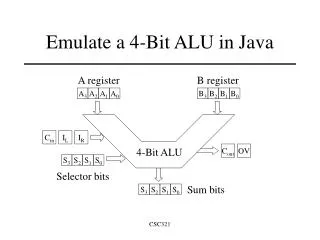
Project Description and ALU Schematic • 1-bit Adder • Four 2 to 1 MUXs • 1 AND and 1 OR gates • Four control inputs, two data inputs.
Longest Path Calculations • Note: All widths are in microns and capacitances in fF
Simulation A – B = 1010 -1011 =1111 Cout = 0 (Borrowed)
Summary • After this project, we became familiar with Cadence tool and the fundamental concepts of IC design. • The total area is = 300um x 320um • The power = 1.3mW • Lessons learned • How to fix the LVS error • Learn how to work in a team • Learn how to make trade offs
Acknowledgements • Thanks to Cadence Design Systems for the VLSI lab • Thanks to Synopsys for Software donation. • Thanks to Professor David Parent.