4-bit ALU
4-bit ALU. Ro berto Reyes S unil Adhikari S amir Patel Y esha Patel. Advisor: Prof. David W. Parent Presentation Date: 12/05/05. Agenda. Abstract Introduction Why Simple theory Project details Schematics Layout Verification: DRC, Extract, LVS Simulation Results Cost Analysis


4-bit ALU
E N D
Presentation Transcript
4-bit ALU Roberto Reyes Sunil Adhikari Samir Patel Yesha Patel Advisor: Prof. David W. Parent Presentation Date: 12/05/05
Agenda • Abstract • Introduction • Why • Simple theory • Project details • Schematics • Layout • Verification: DRC, Extract, LVS • Simulation Results • Cost Analysis • Conclusion • Lessons Learned
Abstract • 4-bit ALU • Gates Used: NAND, XOR, AOI, NOR, INV • Number of Operations: 16-Logic, 16-Arithmetic • Driven load: 30fF • Clock Frequency: 222 MHz • Power Density: 13.54 mW/cm2 • Area: 430.00 x 833.10 µm2 • Specifications: • Frequency: 200 MHz • Max Power: 20W/Cm2
Goal • Design 4-bit ALU using Cadence Tools • Implementation of concepts learned in EE 166 – Design of CMOS Digital Integrated Circuit • To improve the Motorola designing criteria from previous projects
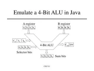
Introduction • ALU is a fundamental unit of many combinational circuits which performs logical and arithmetic operations. • Cadence Tools were used to verify the Design and Simulation. • CMOS Design • high speed • less power
Project Summary • Using particular widths for transistors • Consuming less power than previous designs • Achieving higher operating frequency than previous project • Tried minimizing area compared to the previous projects
Longest Path Gate Level Schematic NC Verilog DRC Layout Transistor Level Schematic Post Extraction LVS Extracted Verify ALU Design Power Check Project Flowchart
Gate Level Schematic S0 S1 S2 S3 B3 G Cn+4 A3 B2 P A2 F3 B1 F2 A1 B0 A=B F1 A0 M F0 Cn
Longest Path Calculations Shortest Path
Function Verification Function Table L = LOW Voltage H = HIGH Voltage * Each bit is shifted to the next most significant position **Arithmetic Operations expressed in 2s complement notation. Table used from http://www.mil.ufl.edu/courses/eel4712/docs/74LS181.pdf
Logic Verification + CK Logic Operation : A B Keeping S3 = H, S2 = L, S1 = L, S0 = H, M= H RSET A0 1 A1 1 A2 0 A3 0 B0 0 B1 0 B2 0 B3 0 F0 1 F1 1 F2 0 F3 0 τplh = 2.64ns τphl = 2.62ns
Logic Verification CK Arithmetic Operation : A + B Keeping S3 = H, S2 = L, S1 = H, S0 = H, M= L, and Cn = L RSET A0 1 A1 1 A2 0 A3 0 B0 0 B1 0 B2 0 B3 0 F0 1 F1 0 F2 1 F3 1
Cost Analysis • Estimated time spent on each phase of the project • Drawing Schematics: 1 week • Verifying Logic : 1 week • Verifying Timing : 1week • DFF Schematic and DFF Layout: 3 days • 4-bit ALU Layout: 2 weeks • Post Extraction of Timing: 4 days
Conclusion • Power Density: 13.54 mW/cm2 • Clock Frequency: 222 MHz • Area: 430.00 x 833.10 µm2 • Metal 1, 2, and 3are used • Hold time: 0.26ns • Setup time: 0.73ns • 902 NMOS & 902 PMOS transistors • 513 Nets • 26 Terminals
Lessons Learned • Do the “Hay” when the sun shines! • Do NOT use prime (‘) to name pins in NC Verilog. • Do NOT cross same type of metals. • Consult your manager instead of being lost. • Good Coordination • Learn to make trade offs
Acknowledgement • Thanks to Professor D. Parent for his guidance and unlimited office hours • Thanks to Synopsys for software donation • Thanks to Cadence Design Systems for the VLSI lab