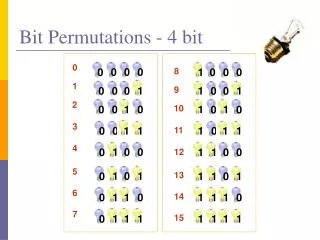
4-Bit ALU
4-Bit ALU. Specifications Functionality: AND, OR , XOR, ADD Maximum propagation delay : 2ns Power budget: 30mW Area: 200 µm ×400µm. Prepared by: Christie Ma, Manjul Mishra, Ka Yung Presented to : Dr. David Parent Date: 7 th May, 2003. Highlights. Introduction- How does the circuit work

4-Bit ALU
E N D
Presentation Transcript
4-Bit ALU SpecificationsFunctionality: AND, OR , XOR, ADDMaximum propagation delay : 2nsPower budget: 30mWArea: 200 µm ×400µm Prepared by: Christie Ma, Manjul Mishra, Ka Yung Presented to : Dr. David Parent Date: 7th May, 2003
Highlights • Introduction- How does the circuit work • Approach for the design • Individual blocks – AND gate, OR gate, XOR gate, Full Adder, and 4-to-1 MUX • Wiring of 1-bit and 4-bit ALU • Verification of functionality – test vectors • Post extracted simulation with propagation delay • Power consumption • Conclusions
Circuit Functionality S1 S0 A0 B0 A0 B0 F0 4:1 MUX A0 B0 A0 B0 C0 ADD Cout0 Block diagram for 1-bit ALU
Block Diagram for 4-Bit ALU S1 S0 A0 B0 C0 1-bit ALU F0 F1 F2 F3 Cout0 A1 B1 1-bit ALU Cout1 A2 B2 1-bit ALU Cout2 A3 B3 1-bit ALU Cout3
Design Flow Sketch schematic according to Boolean Algebra Measure power used Find Euler Path Measure delay time Draw stick diagram Verify functionality Calculate Wn Wp for each block Run DRC, LVS, extracted simulation for 4-bit ALU Run Spice simulation to fix Wn, Wp Route four 1-bit ALUs to form a 4-bit ALU Draw schematic for each block Run DRC, LVS, extracted simulation for 1-bit ALU Layout for small blocks Run DRC, LVS, extracted simulation for small blocks Route small blocks together to form 1-bit ALU
AND2 schematic Wp=5.4 m Wn=15.15 m
OR2 Schematic Wp=8.4m Wp=5.85 m Wn=14.25 m Wn=10.2 m
XOR2 Schematic Y = A xor B = AB’ + A’B = (AB + A’B’)’ AOI21 = (AB + C)’ if C = A’B’ C = (A+B)’ C = A nor B Therefore, using one AOI21 and one NOR gate, we can implement XOR gate without using any INV. Wp=15.9m Wn=23.4m
Full Adder Schematic Wp=6.15m Wn=3.6m Cout=AB+ACin+ BCin = AB+Cin(A+B) Sum= ABCin + (A+B+Cin)Cout’
4-to-1 MUX schematic F0= S1’ S0’Y00+ S1’S0Y01 +S1S0’Y10+S1S0Y11 F0= S0’(S1’Y00+S1Y10)+S0(S1’Y01+S1Y11) Wp=9.9 m 2-to-1 MUX 2-to-1 MUX 2-to-1 MUX Therefore, we need three 2-to-1MUXs to build a 4-to-1 MUX 2-to-1 MUX schematic Wn=6.45 m
4-to-1 MUX Layout 3 One 2-to-1 MUX Three 2-to-1 MUXs to form a 4-to-1MUX
1-bit ALU Layout AND OR XOR ADDER 4-to-1 MUX
4-bit ALU Layout Area = 197m 347.4 m
Test Vectors • Walking ones for inputs on all operations (1-8) • Testing for Cout and Cin (9, 10)
Simulation Results A3 = 1, Ax = 0, Bx = 0
Simulation Results A2 = 1, Ax = 0, Bx = 0
Simulation Results A1 = 1, Ax = 0, Bx = 0
Simulation Results A0 = 1, Ax = 0, Bx = 0
Simulation Results B3 = 1, Ax = 0, Bx = 0
Simulation Results B2 = 1, Ax = 0, Bx = 0
Simulation Results B1 = 1, Ax = 0, Bx = 0
Simulation Results B0 = 1, Ax = 0, Bx = 0
Simulation Results (Cout) A3 = 1, B3 = 1
Simulation Results (Cin) C0 = 1, A0 =1, B0 =1
Propagation Delay for AND gate 274.1ps
Propagation Delay for OR gate 237.9 ps
Propagation Delay for XOR gate 226.7ps
Propagation Delay for Full Adder 495.5 ps
Propagation Delay for 4-to-1 MUX 330.4 ps
Propagation Delay For 4-bit ALU (when S1=S0=0 AND Operation) t F2 = 705.9ps t F3 = 698.2ps
Propagation delay For 4-bit ALU( when S1=0, S0=1 OR Operation) t F3 = 673.2 ps t F2 = 693.8 ps
Propagation Delay for 4-bit ALU(when S1=1, S0=0 XOR Operation) t F3 = 678.7 ps t F2 = 661.2 ps
Propagation Delay for 4-bit ALU (when S1=S0=1 Add Operation) t F1 = 1.383 ns t F0 = 987.9 ps
Propagation Delay for 4-bit ALU (when S1=S0=1 Add Operation) t F3 = 1.949 ns t F2= 1.484 ns
Propagation Delay for 4-bit ALU (when S1=S0=1 Add Operation) t Cout3 = 1.339 ns
Power Simulation for 4-bit ALU (when S1=S0=0 AND Operation) Power = 26.8 mW
Power Simulation For 4-bit ALU( when S1=0, S0=1 OR Operation) Power = 26.69 mW
Power Simulation for 4-bit ALU(when S1=1, S0=0 XOR Operation) Power = 21.38mW
Power Simulation for 4-bit ALU (when S1=S0=1 Add Operation) Power = 23.35mW