Download
1 / 50
500 likes | 707 Vues
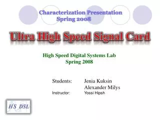
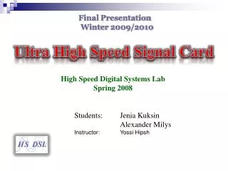
Final Presentation Winter 2009/2010. Ultra High Speed Signal Card. High Speed Digital Systems Lab Spring 2008 Students: Jenia Kuksin Alexander Milys Instructor: Yossi Hipsh. Content. Project Objectives Project Description Block Diagram Elecrical Scheme PCB Design

E N D
Final Presentation Winter 2009/2010 Ultra High Speed Signal Card High Speed Digital Systems Lab Spring 2008 Students: JeniaKuksin Alexander Milys Instructor: YossiHipsh
Content • Project Objectives • Project Description • Block Diagram • Elecrical Scheme • PCB Design • Stackup • Simulation • PCB Assembly • Bugs and fixing • Measurements • Design Proposals
Project Objectives Designing High Speed Transmission Line Board which will provide an ideal vehicle for learning about Signal Integrity issues like: • Reflections in Transmission Lines • Cross Talk in Transmission Lines • Jitter • Skew
Project Description • The purpose of the board is to provide the ideal vehicle for High Speed Phenomena Experiment in High Speed Digital Labaratory. It uses the high speed generarator to expose students to a wide range of SI phenomena as Reflections and Cross Talk in Transmission Lines, • Jitter and Skew .
Experiment Environment Instructor High Speed Transmission Line Board Controller Switching System Pulser Transmission Lines Array Student
Block Diagram Controller S0 0narrow pulse 1wide pulse S3 Connects One channel from 36 To scope S2 Connects One channel from 36 To scope Analog Switches Analog Switches S1 Will be OE for splitters Pulser Signal Splitter Z(Source) Transmission Lines 36 lines Termination Z(Load) 1 36 36 36 S5 Control for MCP195 (jitter)
Description of Main Blocks • Pulser - creates short (0.5-1 nsec) and long (10-13 nsec) pulse signal with very low rise/fall time (200ps) . • Signal Splitter – launching a signal into a transmission line and converts differential signal to single ended while only one line can be alive at the same time • Analog Switches – transmit the measured voltage signal on input/output of selected transmission line to oscilloscope.
Transmission Lines – will contain 36 microstrip, single ended transmission lines with different terminations. • Controller – Based on Altera DE2 Board, controls all of the operation of the High Speed Transmission Line Board.
PCB Design • 8 layers, 25x30cm board dimensions. • High speed data lines, microstrip and stripline formats. • Rise time of signals range from 150ps to 300ps. • Pre and post layout simulations are required. • Multiple onboard power supplies – many local power planes. • Many identical hierarchical blocks on a schematics require efficient layout reuse. • Design is completed in OrCAD PCB Editor
Layout Stackup Total Thickness 101.8 mil
Top Layer Microstrip Lines
Second Layer GND Plane Support for microstrip lines from top layer. Support for Striplines from third layer
Third Layer Striplines and power plane
Forth Layer GND Plane and Power Planes Support for Striplines from third layer
Fifth Layer GND plane Support for Striplines from six layer
Six Layer Striplines
Seven Layer GND Plane and Power Planes
Bottom Layer Microstrip Lines
Pre Layout Simulation Circuit In HyperLynx Simulation of Microstrip Lines without Amplifier Driver: MC100LVEP111 IBIS Model for MC100LVEP111FA 3.3V was downloaded from ON Semiconductor site Load: 250 Ω For the sake of observing reflections.
Pre Layout Simulation results In HyperLynx Desired Signal Without coupling effect For getting clean output signal without interference necessary to get over crosstalk between microstrip line folds. In order to determine the optimal spacing between microstrip line folds the simulation accomplished with several values 203um, 600um, 800um and 1000um.
203um spacing 600um spacing 800um spacing 1000um spacing
From simulation results it is clear that optimal spacing between microstrip line folds is 800 um since no noticeable improvements were seen when increasing to 1000um.
OrCADSigXplorer Simulation Unmatched source termination • Rsource =100ΩRload =20Ω • Rsource =100ΩRload =50Ω • Rsource =100ΩRload =250Ω Matched source termination • Rsource =50ΩRload =20Ω • Rsource =50ΩRload =50Ω • Rsource =50ΩRload =250Ω Crasstalk • 10mil space Unmatched source termination Rsource =15ΩRload =20Ω Rsource =15ΩRload =50Ω Rsource =15ΩRload =250Ω
Top and Bottom Top Bottom
PCB Assembly Working hard Component soldering
Bugs and repairs • Voltage regulator U40 (TPS76650) is replaced with two diodes 1N0007 in parallel after the short circuit current appeared and voltage dropped below 5V. Apparently because of excessive turn on current need by SP6T switches. • LE Input (pin 1) of U36 and U37 (4 to 16 line decoder 74HCT4515) was connected to 5V because when LE is high the selected output is determined by the data on An. • The termination resistors are added to U22 (MC100EP195) in pin 4 and 5 as described in datasheet.
Termination Voltage Vt bug • Voltage regulator for 1.3V was detected as not properly working due to high output currents from PECL outputs that incoming to voltage regulator output and caused it to stop working. The solution was to remove the voltage regulator from the board and connect to the VT current source or power resistor which constrain voltage of 1.3V.
Problem description Vt is the biasing voltage for output stage of PECL circuit. As can be seen, for Biasing condition of output drivers , it will be necessary to source current out of the PECL circuit. This will set a constrain on the power supply that can be connected to the Vtt pin.
Why simple (Linear) Voltage Regulator Cannot be used as Vtt supply. Voltage Regulator (Linear) I Linear (non switching) regulator is always sourcing current it will not be able to provide appropriate current direction for PECL output stage biasing. In order to provide Vtt we need to use regulator with Push-Pull stage, Negative configuration of linear regulator or dynamic current source with constant voltage drop. In order to check the Vtt generation we will use the last option.
Solution for Vt OP1 : LM741 may be used (or any other) Bias LM741 with +/-10v. Latter we will use better opamp with higher output swing and single supply operation. Q1 must be with IDmax>2A If mosfet is not available. BJT might be used , but because of limited output current sourcing of the opampand a power BJT low current gain. We will need to connect two BJTs in darlington configuration , for achieving higher total current amplification. The feedback has to be connected to positive input because of the additional 180deg phase shift caused by the Q1. Vdd + R1 Q1 OP1 - R2 R1/R2 = (Vdd/1.3)-1 R1+R2 >1K Calculate it according resistor availability
Probe Calibration before Measurements Measurements were accomplished with 1156A Active Probe, 1.5 GHz
Signal creation chain OSC One Shot CMOS to ECL And Output Differentiator CM DM Rise/fall times = 200ps Rise/fall times = 200ps DM CM One Shot : T=20.11ns, Ton=9.11ns
50 to 50 measurement Narrow Probe A Probe B 6dB Att. Amp 50ohm Zo = 50 ohm 50ohm Start X End X Test= 3.844-(8.28-7.422)=2.9ns Rise and fall time from 20% to 80%. Tfall (SX) = 266ps Trise (SX) = 400ps Tfall (EX) = 300ps Trise (EX) = 496ps Tfall (PA) = 208ps Trise (PA) = 232ps Tfall (PB) = 312ps Trise (PB) = 328ps 7.422ns 8.28ns 3.844ns 2.94ns 2v End X Probe B Start X Probe A
50 to 0 measurement Narrow Probe A Probe B 6dB Att. Amp 50ohm Zo = 50 ohm 1 ohm Start X End X Scale factor of StartX and EndX is ~10 Scale factor of StartX and ProbeA is ~10 Tfall (SX) = 232ps Trise (SX) = 322ps Tfall (SXsecond) = 433ps Trise (SXsecond) = 496ps Tfall (PA) = 229ps Trise (PA) = 275ps Tfall (PAsecond) = 322ps Trise (PAsecond) = 455ps 7.55ns 7.68ns 7.24ns 7.63ns Probe B End X Start X Probe A
50 to 0 measurement Wide Start X Probe A 7.55ns End X Probe B
15 to 1 measurements 7.533ns 3.76ns 8.8mv 403mv 22.4mv 1.08mv Scale factor of StartX and EndX is ~10 Scale factor of StartX and ProbeA is ~10 281mv 6.2mv 103mv 2.3mv Start X 18.9mv 972mv 3.766ns Probe B 3.711ns Tfall = 222ps Trise = 366ps End X Probe A
50 to 100nH measurements Narrow Tfall (SX) = 244ps Tfall (EX) = 333ps Tfall (PA) = 222ps Trise (PA) = 244ps 3.82ns Probe A Start X 3.83ns 3.42ns Probe B End X
50 to 100nH measurements Wide Start X Probe A Probe B End X
50 to 100pF measurements Narrow Tfall (SX) = 222ps Tfall (SX) = 244ps Tfall (PA) = 246ps Trise (PA) = 265ps 7.511ns 3.75ns 3.644ns
50 to 100pF measurements Wide Probe A Probe B 6dB Att. PECL Amp 50ohm Zo = 50 ohm 100pF Start X End X
Design Proposals Change to switching power supply Add push-pull stage on Vt voltage Change to balanced transformer to converting signals to single ended. Add microcontroller on board with RS232/USB interface to PC and control everything this way. Put sensing to crosstalk input Aggressor line. Several lines can be driven from one source (one AMP) using analog mux to direct the power.
New available module for Differential to Single ended conversion New high frequency transformers allow to convert signal from differential to single ended in a single stage without use of amplifier. Vtt PECL At the design stage, transformers with proper BW was not available.
The End • We want to thank everyone for helping in our project. • YossiHipsh • Eli Shoshan • MonyOrbach • ElaGluzman • Ina Rivkin