Download
1 / 83
840 likes | 1.12k Vues
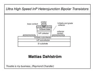
Ultra High Speed InP Heterojunction Bipolar Transistors. Mattias Dahlström. Trouble is my business, (Raymond Chandler). Ultra High Speed InP Heterojunction Bipolar Transistors. Introduction to HBT’s How to make a fast HBT… Delay terms The graded base The base-collector grade

E N D
Ultra High Speed InP Heterojunction Bipolar Transistors Mattias Dahlström Trouble is my business, (Raymond Chandler)
Ultra High Speed InP Heterojunction Bipolar Transistors • Introduction to HBT’s • How to make a fast HBT… • Delay terms • The graded base • The base-collector grade • Recent results • Record fmax mesa DHBT* • Record f DHBT *details regarding this to follow
The transistor Small change in base current large change in collector current Schematic of an HBT Typical common-emittercharacteristics
InP lattice structure Nearest neighbor: 2.5 A Lattice constant: 5.86 A
InP InGaAs InP and InGaAs have G-L separations of ~0.65 eV, vs ~0.4 eV for GaAs→ larger collector velocityInGaAs has a low electron effective mass → lower base transit time
Objectives and approach Objectives:fast HBTs → mm-wave power, 160 Gb fiber opticsdesired: 440 GHz ft & fmax,10 mA/mm2, Ccb/Ic<0.5 ps/Vbetter manufacturability than transferred-substrate HBTsimproved performance over transferred-substrate HBTs Approach: narrow base mesa → moderately low Ccb very low base contact resistance required, and good alignment → carbon base doping, good base contact process high ft through high current density, thin layers bandgap engineering: small device transit time with wide bandgap emitter and collector
Potential uses of InP HBT Communication systems: • wireless communication, fiber optics transceivers, • digital processing in radar (ADCs, DACs) Types of circuits: • broadband amplifiers, power amplifiers, laser/modulator drivers • comparators, latches, fast logic Circuit characteristics • 1-10 000 HBTs per IC • Very high demands for speed (40-200 GHz) • Fast logic with moderate power consumption (~20 mW/gate) • Moderate Output Power mmwave power amps, optical modulator drivers ~6 V at Jc=4 mA/μm2 , ~2 V at Jc=8 mA/μm2
DHBT band diagram: under bias emitter collector base
High speed HBT: some standard figures of merit • Small signal current gain cut-off frequency (from H21) • Maximum power gain ( from U) • Collector capacitance charging time when switching :
Scaling laws for fast HBTs for x 2 improvement of all parasitics: ft, fmax, logic speed…base Ö2: 1 thinnercollector 2:1 thinneremitter, collector junctions 4:1 narrowercurrent density 4:1 higheremitter Ohmic 4:1 less resistive transferred-substrate Challenges with Scaling:Collector mesa HBT: collector under base Ohmics. Base Ohmics must be one transfer lengthsets minimum size for collector Emitter Ohmic: hard to improve…how ?Current Density: dissipation, reliabilityLoss of breakdownavalanche Vbr never less than collector Eg (1.12 V for Si, 1.4 V for InP) ….sufficient for logic, insufficient for power narrow collector mesa
Contact resistance: tunneling through barrier Theory: idealized contact • High doping: 1-9 1019 cm-3 • Small bandgap: InAs<InGaAs<InP<GaN • Surface preparation: no interstitial oxide • Metal reactions
Pd-based contacts Ohmic contact to p-type material 10-100 times worse than n-type. Work function line-up, electron/hole effective mass • Pd/Pt reacts with III-V semiconductor: • InGaAs+Pd As + (In,Ga)Pd+(In,Ga)(Pd,As) • Pd reaction depth ~4 x thickness • 25 Å Pd for 300 Å base • Contact resistance: • 100-500 -m21-20 -m2 • from TLM and RF-extraction Yu, J.S.; Kim, S.H.; Kim, T.I. ‘’PtTiPtAu and PdTiPtAu ohmic contacts to p-InGaAs’’, Proceedings of the IEEE Twenty-Fourth International Symposium on Compound Semiconductors, San Diego, CA, USA, 8-11 Sept. 1997
Emitter resistance: grades removed InGaAs cap layer InP emitter light doping Contact resistance: 50 m2 25 m2 15 m2 High doping 3 1019 cm-3 No InGaAs-InP grade necessary at very high doping Thin undepleted n- emitter Small emitter area increases Rex heavy doping At degenerate doping levels grades are not necessary
Base resistance TLM measurement Rbb is a critical parameter for fmax, and in npn HBT the base contact resistance dominates. Rbb is minimized through high base doping and improved base contact metallization, small undercut Wgap, and long emitter Le
Problems with very thin bases • Etching and depletion effects reduce the effective base thickness Tb, and increases the base resistance. • At 500 nm scaling generation, best base thickness is 30-40 nmbetter fmax , lower Rbb-related delay terms in gate delay ,minimal improvement in ft between 25 & 30 nm High resistance
Increase of sheet resistance with thin base layers Rb,extrinsic=800-1000 Ω/sq Rb,intrinsic=600-750 Ω/sq Base surface exposed : InGaAs base doped 6 1019 cm-3, surface pinned at 0.18 eV. Surface depletion decreases base thickness 40 Å. Base protected by E/B grade (contacts diffused through 160 Å grade) Surface depletion Wet etching
Collector resistance Rc: access resistance between collector contact and the mesa. Minimized by large collector contacts, and low resistance subcollector
Tsubc Subcollector design Goals: • minimize electrical resistance • minimize thermal resistance • limit thickness to improve manufacturability Thermal conductivity of InGaAs ~5 W/mK Thermal conductivity of InP ~68 W/mK Etch stop layer provides collector undercut – less Cbc Some still use all InGaAs subcollector… Subcollector resistivity 500 A InGaAs + 2000 A InP ~ 11 /sq 125 A InGaAs + 3000 A InP ~ 9 /sq - 53 % of thermal resistance Etching selectivity of InGaAs vs. InP main limit 50 A InGaAs Contact resistance better to 125 A than 50 A after annealing
Base-emitter capacitance Cje is the junction capacitance between the emitter and base Cje corresponds to ~100 Å depletion thickness Minimized by shrinking the emitter area at fixed or at increasing current Ic
Base-collector capacitance Cbc is the junction capacitance between the base and subcollector.
Base-collector capacitance Collector thickness reduced due to speed requirements: Breakdown limits thickness Ccb increases ! • Tc = 3000 A 2150 A 1500 A • Abc must be kept small: • narrow emitter • narrow base contacts • undercut of base contacts • implant or regrowth
is 10-50 Theory of the base If gain is limited by Auger recombination in the base: The base sheet resistance: The base transit time: • Decreasing increases . • High Na and Tb for low s decreases • Grade gives 30-50 % improvement ps is 400-900 /sq is 100-250 fs
Base Transit Time Fitting of relevant parameters of the form Kroemer’s double integral: Drift-Diffusion equation for base current: With doping as Intrinsic carrier concentration Exit term Diffusivity Ballistic injection: Solution used for evaluation of the base transit time:
Base grading Graded bandgap Graded doping Change in In:Ga ratio InAs: Eg=0.36 eV GaAs: Eg=1.43 eV Doping 8 5 1019 cm-3
Base grading: induced electric field Limits: Bandgap narrowing, needs degenerate doping Limits: strain Induced electric field accelerates electrons towards collector – decreases base transit time and increases gain
The effect of degenerate doping Strong variation in Fermi-level with doping at high doping levels Evidence: Observed Vbe increase Von~ φbi , increases with Ev Nb=4 1019cm30.75 V Nb=8 1019cm30.83 V for graded base-emitter
Base bandgap narrowing Bandgap grade Doping grade Model after V. Pavlanovski BGN provides an electric field opposing the doping-induced field. ~1:5 in magnitude
Base Transit time Ballistic effects may arise when Tb<180-200 @5 1019 cm-3 (Tessier, Ito) Bandgap grade and doping grade give same b Results: Bandgap graded Doping graded DC gain 25 18 ft 250 GHz 282 GHz
Grade No Grade Collector design Transit time: Close inspection show velocity near base most important • Use grade • Use setback
Base-collector grade • Early grade designs: • Too coarse • No setback layer Gain: 7 f: 128 GHz (Tc=3000 A) Jkirk: 1.3 mA/μm2 • Recent grade designs: • 15 A period • 200 A setback layer Gain: 27 f: 282 GHz (Tc=2150 A) Jkirk: 4 mA/μm2
InAlAs/InGaAs super lattice • Why super lattice? • MBE is more suited for super lattice than quaternaries. • InP/InGaAs gives poor quality material due to phosphorous-arsenic intermixing • MOCVD growth → InGaAsP grade • GaAsSb base needs no grade
Quantum mechanical trapping in grade • Quantum well trapping • Electron/hole in the InGaAs well • 500 meV InAlAs potential barrier • A rough approximation: the infinite potential well. If En> 500 meV (InGaAs/InAlAs potential) no electron confinement ~31 A is the maximum allowed InGaAs width by this model
The delta-doping H. Kroemer : a conduction band difference can be offset with a grade and a delta-doping No delta-doping Delta-doping Vbc=0.3 V Vbc=0.3 V With this choice the conduction band will be smooth
The setback layer • An InGaAs layer beneath the base • Margin for Base dopant diffusion • Increases Electron speed at SL No setback Setback Vbc=0.3 V Vbc=0.3 V
Collector design: velocity and scattering Collector band profile designed for greatestpossible distance without G-L scattering G-L scatteringpossible No G-L scattering
Collector under current (simulation) Current blocking Nc reduced by Jc/q/vsat
Metal resistance • Resistance of e-beam deposited metals higher than “book” values. • Metal resistance increases when T<1000 A • TiPdAu 200/400/9000 A • PdTiPdAu 30/200/400/600 A • TiPdAu 200/400/4000 A Reduces fmax Thermal stability? Problem for base contact (PdTiPdAu with 600 A gold) sm=0.5 Ω/sq 3-8 Ω added to Rbb
Results • 2150 A collector high fmax, high Vbr,CEO IPRM 2002, Electron Device Letters, Jul. 2003; M. Dahlström et al, ''Ultra-Wideband DHBTs using a Graded Carbon-Doped InGaAs Base'' • 1500 A collector high f, high fmax ,high Jc Submitted to DRC 2003; M. Dahlstrom, Z. Griffith et al.,“InGaAs/InP DHBT’s with ft and fmax over 370 GHz using Graded Carbon-Doped Base”
InGaAs 3E19 Si 400 Å InP 3E19 Si 800 Å InP 8E17 Si 100 Å InP 3E17 Si 300 Å InGaAs graded doping 300 Å Setback 2E16 Si 200 Å Grade 2E16 Si 240 Å InP 3E18 Si 30 Å InP 2E16 Si 1700 Å InP 1.5E19 Si 500 Å InGaAs 2E19 Si 500 Å InP 3E19 Si 2000 Å SI-InP substrate High fmax DHBT Layer Structure and Band Diagram Emitter Collector Base Vbe = 0.75 V Vce= 1.3 V • 300 A doping graded base • Carbon doped 8*10195* 1019 cm-2 • 200 Å n-InGaAs setback • 240 Å InAlAs-InGaAs SL grade • Thin InGaAs in subcollector
InGaAs 3E19 Si 400 Å InP 3E19 Si 800 Å InP 8E17 Si 100 Å InP 5E17 Si 400 Å InGaAs graded doping 300 Å Setback 3E16 Si 200 Å Grade 3E16 Si 240 Å InP 3E18 Si 30 Å InP 3E16 Si 1030Å InP 1.5E19 Si 500 Å InGaAs 2E19 Si 125Å InP 3E19 Si 3000Å SI-InP substrate High f DHBT Layer Structure and Band Diagram Emitter Collector Base Vbe = 0.75 V Vce= 1.3 V • Thinner InP collector • Collector doping increased to 3 1016 cm-3 • Thinner InGaAs in subcollector • Thicker InP subcollector
Results: DC High fmax DHBT High f DHBT Gain: 23-28 nb/nc: 1.05/1.44 Vbr,CEO: 7 V Gain: 8-10 nb/nc: 1.04/1.55 Vbr,CEO:4 V No evidence of current blocking or trapping
Results: RF High fmax DHBT High f DHBT • Highest fmax for mesa HBT • Highest f for mesa DHBT • Highest (f, fmax)for any HBT • High current density
Results: Base width dependence Emitter junction 0.6 x 7 m, Vce=1.3 V Tb=300 A. Tc=1500 A
Results: RF - trends Variation of f vs. Ic and Vce , of an HBT with a 0.54 m x 7.7 m emitter, and a 2.7 m width base-collector junction. Variation of f and fmax vs. Vce, of an HBT with a 0.54 m x 7.7 m emitter, and a 2.7 m width base-collector junction. Ic=20 mA. Need higher Vce for high current f drops at high Vce high Vce for full collector depletion
Results: evolution f fmax Old grade Final grade New grade Jopt Strong improvement in f and Jopt f and fmax > 200 GHz at Jc >10 mA/m2 Tc =1500 A
Capacitance vs. current DHBT 17 Abrupt emitter base junction DHBT 20 Graded emitter base junction Jmax~3 mA/m2 Jmax~6.5 mA/m2 Emitter junction 0.54x7.6 um and 0.34x7.6 um. Tc= 2150 A, Nc=2 1016 cm-3 Emitter junction 0.5x7.6 um Tc= 1500 A, Nc=3 1016 cm-3 48 % Jmax~3.2 mA/m2 for Tc=2150 A
E We B B Vce=1.5 V C Vce=1.3 V Wbc Area dependence on capacitance reduction Ccb from Y-parameters at 5 GHz Ccb is reduced where the current flows reduce extrinsic base Extrapolating with linear fit gives 55 % for r=1
Max current density vs. emitter size The current at which Ccb increases (Jmax) as a function of emitter width for two different HBT • Narrow emitters have higher critical current density • Not necessarily higher ft (due to Rex) - Current spreading