Matching Bipolar Transistors
Matching Bipolar Transistors. Younghoon Song Nghia Nguyen Hanna Kim Eyad Fanous Steven Hsu Kei Wong. Introduction.

Matching Bipolar Transistors
E N D
Presentation Transcript
Matching Bipolar Transistors Younghoon Song Nghia Nguyen Hanna Kim Eyad Fanous Steven Hsu Kei Wong
Introduction • Matchingis the statistical study of the differences in the electrical parameters between identically designed components placed at a small distance in an identical environment and used with the same bias conditions • Reason for the study of the matching properties of transistors • - Mismatch can seriously affect the performance of analog and digital CMOS integrated circuits • - Matching determines the homogeneity in the response of equally laid out circuits
Matching Bipolar Transistors • Bipolar transistors can be difficult to match when different sizes and shapes are involved. • Most bipolar transistor circuits use simple integer ratios.
Matching Bipolar Transistors • Transistors that have identical dimensions and operating at equal current densities do not operate at identical base emitter voltages. • The differences in the base emitter voltage is called Offset Voltage.
Matching Bipolar Transistors Offset Voltage is denoted by VBE VBE = VT ln (Is1/Is2) • VT is the threshold voltage which is 26mv at 300° K • Is1 and Is2 is the emitter saturation currents of the two transistors. • 1% variation in emitter area produces 0.25mV of offset
Mismatch Sources • Random Effects - All the stochastic effects such as dopant fluctuations, local mobility fluctuations, polysilicon gate granularity, oxide charges and interface states fluctuations • Systematic and Environment effects - All the technological and geometrical effects which can give origin to a systematic difference between the two transistors in the matched pair
Random Variations The area to periphery ratio • Rap=Kr (Ae^.5) • Rap has the dimensions of the emitter area • Ae is the emitter area • Kr is a dimensionless constant • .250 for squares • .274 for octagons • .282 for circles.
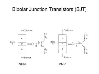
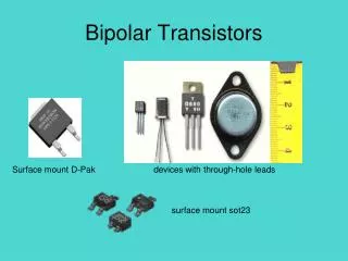
Random Variations Match Bipolar Transistors have three typical emitter geometries. Squares, Octagons, Circles. Figure 1 Examples of NPN transistors
Random Variations Circular Emitters Advantage • largest area to periphery ratio Disadvantage • Circles are approximated as many sided polygons
Random Variations Square Emitters Advantage • Can be rendered precisely on the Photomask Disadvantage • Lower area to periphery ratio
Random Variations Octagonal Emitter Advantage • No approximations while rendering to the photomask • Larger area to periphery than squares Disadvantage • Lower area to periphery than circles
Random Variations • s is the standard deviation between a pair of transistors due to the peripheral and areal fluctuations. • The forumla s is
Emitter Degeneration • Used when bipolar transistors do not match well together • This technique transfers the burden of matching transistor to a set of resistors
Emitter Degeneration • Improves the overall matching of the circuit • Increases the output resistance of the bipolar transistors
Emitter Degeneration • Mismatch between collector currents of two matched bipolar transistors operating at different base collectors voltage can be found with this formula ~ ~
NBL Shadow • NBL Shadow is surface discontinuities caused by oxidation during the NBL anneal propagate upward during epitaxial deposition.
NBL Shadow • NBL shadow causes mismatch between two transistors when it intersects the emitter of a vertical NPN transistor.
NBL Shadow • Several ways to prevent pattern shift from causing mismatches. 1. Replacing the multiple-emitter transistor QA with two single-emitter transistors that are identical to QB. - Problem: Pattern distortion can also produce random variations in the NBL shadow.
NBL Shadow 2. Laying out transistors in a CEB array in which the main axis of symmetry lies parallel to the direction of pattern shift if the direction of pattern shift is known.
NBL Shadow 3. Oversizing NBL to prevent intersection of NBL and emitter if the direction of pattern shift is not known.
NBL Shadow • Lateral PNP transistors generally do not suffer from mismatches caused by the NBL shadow. The width of the collector usually suffices to prevent the shadow from intruding into the base region.
Thermal Gradients • Bipolar ransistors are extremly sensitive to thermal gradients. • Matched bipolar transistors are often used to construct • Differential pairs • Ratioed pairs • Ratioed quads
Thermal Gradients • Differential pair • Is located and constructed for the input stages of amplifiers and comparators to minimize their sensitivity to thermal variations.
Thermal Gradients • Usually employs the two-dimensional common-centroid layout. Cross coupled quad bipolar transistors
Thermal Gradients • Ratioed pair • Makes the voltage proportional to absolute temperature (VPTAT) linear with temperature and independent of current over a wide range of operating conditions. Vbe = Vt ln(A1) A2 A1and A2are the emitter areas of transistors Q1and Q2
Thermal Gradients • Ratioed quad(a variation on the ratioed pair) • Provides a much larger VBE than a simple ratioed pair. • The layouts of ratioed pairs and ratioed quads must provide a high degree of symmetry in a compact layout. VBE = VT ln(A1A2) A3A4 A1to A4are the emitter areas of transistors Q1to Q4
Thermal Gradients • Two common-centroid layouts frequenly used for constructing ratioed pairs.
Stress Gradients • Assembled ICs Experience Stress • Mechanical Stress • Altering Base-Emitter Voltages • Vary Depending on the Bandgap Voltage and Stress • Reducing Betas • Lower Beta Due to Mobility Variations Induced by Piezoresistivity • The Residual Stresses After Molding Process Cause the Base-Emitter Voltages of Bipolar Transistors to Shift and Produce Offsets Between Matched Pairs of Devices
Stress Gradients • Common-Centroid Layout • Techniques to Reduce Stress • Move the Matched Transistors Closer Together • Equalize Stress • Matched Transistors Should Reside in Low-Stress Regions of the Die • Samples Are Shown Below:
Rules For Bipolar Transistor Matching • Minimal Matching • Three-Sigma Offset Voltages of +-1mV or Collector Current Mismatches of +-4% • Moderate Matching • Three-Sigma Offset Voltages of +-0.25mV or Collector Current Mismatches of +-1% • Precise Matching • Three-Sigma Offset Voltages of +-0.1mV or Collector Current Mismatches of +-0.5%
Rules for Matching NPN Transistors • Use Identical Emitter Geometries • The Emitter Diameter Should Equal 2 to 10 Times the Minimum Allowed Diameter • Maximize the Emitter Area-to-Periphery Ratio • Place Matched Transistors in Close Proximity
Rules for Matching NPN Transistors • Keep the Layout of Matched Transistors as Compact as Possible • Construct Ratioed Pairs and Quads Using Even Integer Ratios Between 4:1 and 16:1 • Place Matched Transistors Far Away from Power Devices • Place Matched Transistors in Low-Stress Areas
Rules for Matching NPN Transistors • Place Moderately or Precisely Matched Transistors on Axes of Symmetry of the Die • Do Not Allow the NBL Shadow to Intersect Matched Emitters • Place Emitters Far Enough Apart to Avoid Interactions
Rules for Matching NPN Transistors • Increase the Base Overlap of Moderately or Precisely Matched Emitters • Operate Matched Transistors on the Flat Portion of the Beta Curve • The Contact Geometry Should Match the Emitter Geometry • Consider Using Emitter Degeneration
Rules for Matching Lateral PNP Transistors • Use Identical Emitter and Collector Geometries • Use Minimum-Size Emitters for Matched Transistors • Field-Plate the Base Region of Matched Lateral PNP Transistors • Split-Collector Lateral PNP Transistors Can Achieve Moderate Matching
Rules for Matching Lateral PNP Transistors • Place Matched Transistors in Close Proximity • If Possible, Avoid Constructing VPTAT Circuits from Ratioed Lateral PNP Transistors • Place Matched Transistors Far Away from Power Devices
Rules for Matching Lateral PNP Transistors • Place Matched Transistors in Low-Stress Areas • Place Moderately or Precisely Matched Transistors on Axes of Symmetry of the Die • Do Not Allow the NBL Shadow to Intersect the Base Region of a Lateral PNP
Rules for Matching Lateral PNP Transistors • Operate Matched Lateral PNP Transistors Near Peak Beta • The Contact Geometry Should Match the Emitter Geometry • Consider Using Emitter Degeneration

