Programmable Implementation Technologies
Programmable Implementation Technologies. Introduction. Digital circuit design & implement the circuit on a physical device How do we get from design to IC (integrated circuit, aka chip)? . B. elt. W. a. r. n. k. p. w. s. IC. (a) Digital circuit design.


Programmable Implementation Technologies
E N D
Presentation Transcript
Introduction • Digitalcircuitdesign & implement the circuit on a physical device • How do we get from design to IC (integrated circuit, aka chip)? B elt W a r n k p w s IC (a) Digital circuit design (b) Physical implementation on an IC
a ( ) Belt W a r n k p w s c ( ) b ( ) FPGA company Custom ASIC IC FPGA IC Types, Design Flows • Many IC types • Some fast but expensive • Others cheaper but slower • Types also differ in design flow • Some long time • Others off-the-shelf
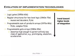
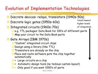
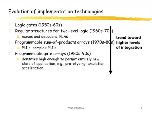
(months) Manufactured IC Technologies • Designer can manufacture a new IC • Months of time, millions of dollars • (1) Full-custom IC • Convert design to layout: Describes location/size of every transistor on IC • Typically created by CAD tools • Send to fabrication plant (fab) to convert layout to actual IC • Photographic, laser, chemical equipment • Hard! • Fab setup costs ("non-recurring engineering", or NRE) high—millions of dollars • Long fab time (months) • Error prone (several "respins") • Uncommon • Only special ICs that demand the very best performance or the very smallest size/power Belt W a r n k k p w w p s s
(1–3 months : cells and wi r ing) Manufactured IC TechnologiesStandard Cell ASIC • (2) Semicustom IC (ASIC) • "Application-specific" IC • (2a) Standard cell ASIC • Pre-layed-out standard-sized "cells" exist in library • Designer instantiates cells into pre-defined rows, and connects • Vs. full custom • Con: Bigger/slower circuit • Pro: Easier/faster to design/manufacture Belt W a r n k p w Cell lib r a r y s w k p cell r o w s cell r o w cell r o w
ab a'b ab' Manufactured IC TechnologiesStandard Cell ASIC • Example: Mapping half-adder to standard cell ASIC co = ab s = a'b + ab' Cell lib r a r y co a s b cell row cell row cell row
( w eeks : just wi r ing) Manufactured IC TechnologiesGate Array ASIC • (2b) Gate array ASIC • "Structured" ASIC • Array of gates already layed out on chip • Just need to wire them together • Vs. standard cell ASIC • Con: Even bigger/slower circuit • Pro: Even easier/faster to design/manufacture • Very popular Belt W a r n k p w s k p w s
a'b ab' Manufactured IC TechnologiesGate Array ASIC • Example: Mapping a half-adder to a gate array ASIC Half-adder equations: s = a'b + ab' co = ab a c o ab b s G a t e a r r a y
Off-the-Shelf Programmable Ics • Manufactured IC technologies require months to fabricate • Also large (million dollar) NRE costs • Programmable ICsare pre-manufactured • User just downloads bits into device, in just seconds • Slower/bigger/more-power than manufactured ICs • But get it today, and no NRE costs
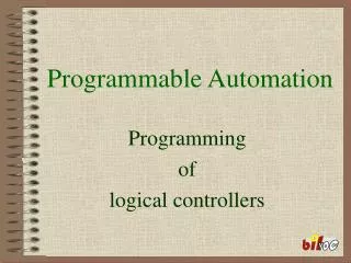
SPLD 1 2 3 I I I • Simple Programmable Logic Devices (SPLDs) • Developed 1970s (thus, pre-dates FPGAs) • Prefabricated IC with large AND-OR structure • Connections can be "programmed" to create custom circuit • Programmable circuit shown can implement any 3-input function of up to 3 terms • e.g., F = abc + a'c' O1 PLD C I programmable nodes
1 2 3 I I I O1 PLD C I programmable nodes Programmable Nodes in an SPLD • Fuse based – "blown" fuse removes connection • Memory based – 1 creates connection p r o g r ammable node Fuse based ( a ) F use "unbl o wn" fuse "bl o wn" fuse Memory based mem mem 1 0 ( b )
k p s B elt W a r n k kps' p w × × w s × × × × × × PLD C I PLD Drawings and PLD Implementation Example 1 2 3 I I I • Common way of drawing PLD connections: • Uses one wire to represent all inputs of an AND • Uses "x" to represent connection • Crossing wires are not connected unless "x" is present wired AND * 3 2' I I × × O1 PLD C I • Example: Seat belt warning light using SPLD × × × 0 0 Two ways to generate a 0 term
Off-the-Shelf Programmable ICFPGA • Popular programmable IC–FPGA • "Field-programmable gate array" • Developed late 1980s • Though no "gate array" inside • Named when gate arrays were popular in 1980s • Programmable in the "field" (e.g, your lab) rather than requiring a fab
F = x'y' + xy 4x 1 Mem. 4x 2 Mem. G = xy' 4x 1 Mem. 1 rd 1 rd x y F G 1 rd 0 1 0 10 0 1 1 0 0 1 0 1 0 1 00 1 0 0 1 0 0 2 0 2 01 2 0 1 0 0 1 x=0 3 1 3 10 3 1 a1 a1 x a1 x 1 1 1 0 a0 a0 y a0 y D D1 D0 D y=0 F=1 F F G FPGA Internals: Lookup Tables (LUTs) • Basic idea: Memory can implement combinational logic • Ex: 2-address memory can implement 2-input logic • 1-bit wide memory – 1 function; 2-bits wide – 2 functions • Such memory in FPGA known as lookup table (LUT) F = x'y' + xy x y F 0 0 1 0 1 0 1 0 0 1 1 1
Belt W a r n k p s w k 0 0 0 0 p w 0 0 1 0 0 1 0 0 0 1 1 0 s 1 0 0 0 1 0 1 0 1 1 0 1 8x1 Mem. 1 1 1 0 0 0 1 0 2 0 Pro gr amming 3 0 (seconds) k a2 4 0 p a1 5 0 s a0 6 1 7 0 F ab D IC w Mapping a Combinational Circuit to a LUT
a 512x 1 M em. 3x1 b c d e 3x1 3x1 F f 8x 1 M em. g h 3x1 i ( b ) ( c ) Partitioned among 3x1 LUTs Requires only 4 3-input LUTs (8x1 memories) – much smaller than a 9-input LUT (512x1 memory) FPGAs More Efficient With Numerous Small LUTS • Lookup tables become inefficient for more inputs • 3 inputs only 8 words 8 inputs 256 words 16 inputs 65,536 words! • FPGAs thus have numerous small (3, 4, 5, or even 6-input) LUTs • If circuit has more inputs, must partition circuit among LUTs • Ex: 9-input circuit more efficient on 8x1 mems rather than 512x1 a b c d e F f g h i ( a ) Original 9-input circuit
Sub-circuits have only 3-inputs each kps' 8x 1 Mem. 8x 1 Mem. BeltWarn k 0 0 0 0 p x 1 0 1 1 w 2 0 2 1 s 3 0 3 1 x t k a2 a2 4 0 4 1 p a1 a1 d 5 0 5 1 s a0 a0 6 1 6 1 x+t+d 3 inputs 3 inputs 7 0 7 1 1 output 1 output D D x=kps' w=x+t+d t d Partition circuit into 3-input sub-circuits w Circuits Must be Partitioned among Small LUTs • Example: Extended seat-belt warning light system • (Assume for now we can create any wires to/between LUTs) BeltWarn k p w s t d 5-input circuit, but 3-input LUTs available Map to 3-input LUTs
0 0 0 1 0 0 1 0 0 1 0 0 1 a 0 0 1 b c 0 0 1 3 2 1 0 1 0 1 1 e f Mapping a Circuit to 3x1 LUTs 8x1 Mem . 8x1 Mem . 8x1 Mem . 0 0 0 a a 1 1 1 b b t 2 2 2 c c Y Y 3 3 3 d d a2 a2 a2 4 4 4 a1 a1 a1 u 5 5 5 e e a0 a0 a0 f f 6 6 6 7 7 7 D D D u Y t d • Divide circuit into 3-input sub-circuits • Map each sub-circuit to 3x1 LUT • (Assume for now that we can create any wires to/between LUTs)
0 0 0 1 0 1 0 1 0 0 0 0 1 0 0 0 x t Underutilized LUTs are Common 8x1 Mem . 8x1 Mem . 0 0 1 1 k k 2 2 p p x 3 3 0 s s k a2 a2 w w 4 4 a1 a1 p t t 5 5 s a0 a0 6 6 Sub-circuit has only 2 inputs 7 7 D D w Italics: contents don’t matter
10 00 01 00 Sub-circuit has 2 inputs, 2 outputs 00 10 00 01 0 0 00 00 i1 00 00 i0 00 00 Sub-circuit has 2 inputs, 2 outputs 00 00 Mapping to 3x2 LUTs • Example: Mapping a 2x4 decoder to 3-input 2-output LUTs d0 8x 2 Mem. 8x 2 Mem. 0 0 d1 1 1 2 2 d2 3 3 a2 a2 4 4 a1 a1 d3 5 5 a0 a0 6 6 7 7 D1 D0 D1 D0 i1 i0 d0 d1 d2 d3
0 0 0 0 0 0 1 0 0 0 0 0 0 0 1 0 a 0 0 0 0 a 1 b b 0 0 1 0 2 t c c 3 1 0 0 1 0 2 d 0 1 1 0 F 3 e t d (Note: decomposed one 4-input AND input two smaller ANDs to enable partitioning into 3-input sub-circuits) F e Second column unused; first column implements AND/OR sub-circuit First column unused; second column implements AND More Mapping Issues • Gate has more inputs than does LUT Decompose gate first • Sub-circuit has fewer outputs than LUT Just don't use output a 8x 2 Mem. 8x 2 Mem. b c 0 0 d 1 F 1 2 2 e 3 3 a2 a2 4 4 a1 a1 5 5 a0 a0 6 6 7 7 D1 D0 D1 D0
Switch 2-bit mem . mat r ix s1 s0 m0 i0 m1 o0 i1 4x1 m2 d i2 m ux m3 i3 2-bit mem . s1 s0 i0 Switch o1 i1 4x1 mat r ix d i2 m ux m0 o0 i3 m1 o1 m2 ... o2 m3 2-bit mem . o2 Li ke wise f or o2.. . FPGA Internals: Switch Matrices • Previous slides had hardwired connections between LUTs • Instead, want to program the connections too • Use switch matrices (also known as programmable interconnect) • Simple mux-based version – each output can be set to any of the four inputs just by programming its 2-bit configuration memory FPGA 8x2 Mem . 8x2 Mem . 0 00 0 00 1 00 1 00 2 00 2 00 3 00 3 00 P0 a2 a2 4 00 4 00 a1 a1 P1 5 00 5 00 a0 a0 P2 6 00 6 00 7 00 7 00 D1 D0 D1 D0 Q0 Q1 P3 P4
These bits establish the desired connections Ex: FPGA with Switch Matrix • Mapping the extended seatbelt warning light circuit onto an FPGA with a switch matrix FPGA Switch 11 mat r ix 8x2 Mem. 8x2 Mem. 0 0 0 0 0 0 0 0 s1 s0 m0 1 0 0 1 0 1 i0 m1 o0 i1 4x1 2 2 0 0 0 1 m2 d i2 mux 0 3 3 m3 0 0 0 1 i3 k P0 a2 a2 4 4 00 0 0 a1 a1 p P1 x (kps') 5 5 00 0 0 a0 a0 s P2 00 t 6 6 00 0 1 7 7 00 0 0 s1 s0 i0 Switch D1 D0 D1 D0 o1 i1 4x1 mat r ix d i2 mux Q0 w m0 11 o0 o0 i3 m1 Q1 00 o1 o1 m2 t P3 ... o2 o2 10 m3 10 0 P4 o2 Li Li ke ke wise wise f f or o2... or o2...
Configurable Logic Blocks (CLBs) • Include flip-flops to support sequential circuits • Muxes programmed to output registered or non-registered LUT output FPGA CLB CLB 8x2 Mem . 8x2 Mem . 0 00 0 00 1 00 1 00 2 00 2 00 3 00 3 00 P0 a2 a2 4 00 4 00 a1 a1 P1 5 00 5 00 a0 a0 P2 6 00 6 00 7 00 7 00 CLB output D1 D0 D1 D0 flip-flop 1-bit 1 0 1 0 1 0 1 0 0 0 0 0 CLB output Switch 2x1 2x1 2x1 2x1 configu r ation mat r ix Q0 memo r y m0 o0 00 m1 Q1 o1 00 m2 P3 o2 00 m3 P4
00 00 01 01 00 01 01 01 00 10 01 11 10 11 11 01 Sequential Circuited Mapped to FPGA FPGA CLB CLB 8x2 Mem. 8x2 Mem. 0 0 1 1 2 2 3 3 v P0 a2 a2 a u u 4 4 a1 a1 b P1 d d d 5 5 c a0 a0 P2 6 6 7 7 a t b u D1 D0 D1 D0 c F v t c c G v 1 0 1 0 1 0 1 0 1 1 0 0 Switch x × × × 2 1 2 1 2 1 2 1 d mat r ix F Q0 m0 o0 00 v m1 Q1 G u 01 o1 m2 d P3 o2 10 m3 P4
FPGA Internals: Overall Architecture • Consists of hundreds or thousands of CLBs and switch matrices (SMs) arranged in regular pattern on a chip Connections for just one CLB shown, but all CLBs are obviously connected to channels Represents channel with tens of wires CLB CLB CLB SM SM CLB CLB CLB SM SM CLB CLB CLB
Bit file contents : 00000010 01010101 1 1 00 01 10 00001111 01110111 0 0 Programming an FPGA • All configuration memory bits are connected as one big shift register • Known as scan chain • Shift in the "bit file" of the desired circuit FPGA CLB CLB Pin 8x2 Mem . 8x2 Mem . Pclk 0 0 0 0 0 0 1 0 1 1 0 1 2 0 1 2 0 0 3 0 1 3 0 1 v P0 a2 a2 u 4 1 0 4 0 0 a1 a1 P1 d 5 1 1 5 0 1 a0 a0 P2 6 1 1 6 1 0 7 1 1 7 0 1 D1 D0 D1 D0 v 1 0 1 0 1 0 1 0 1 1 0 0 Switch 2x1 2x1 2x1 2x1 mat r ix Q0 m0 o0 00 m1 Q1 01 o1 m2 P3 o2 10 m3 P4
More on PLDs • Originally (1970s) known as Programmable Logic Array – PLA • Had programmable AND and OR arrays • AMD created "Programmable Array Logic" – "PAL" (trademark) • Only AND array was programmable (fuse based) • Lattice Semiconductor Corp. created "Generic Array Logic – "GAL" (trademark) • Memory based • As IC capacities increased, companies put multiple PLD structures on one chip, interconnecting them • Became known as Complex PLDs (CPLD), and older PLDs became known as Simple PLDs (SPLD) • GENERALLY SPEAKING, difference of SPLDs vs. CPLDs vs. FPGAs: • SPLD: tens to hundreds of gates, and usually non-volatile (saves bits without power) • CPLD: thousands of gates, and usually non-volatile • FPGA: tens of thousands of gates and more, and usually volatile (but no reason why couldn't be non-volatile)
FPGA-to-Structured-ASIC • FPGA sometimes used as ASIC prototype • Typical flow • (1) Implement user circuit on FPGA and test • (2) Implement user circuit on ASIC (large NRE cost) • FPGA-to-structured-ASIC flow • (1) Implement user circuit on FPGA and test • (2) Implement FPGA on ASIC • ASIC reflects FPGA structure, NOT the user's circuit structure • But remove programmability—LUTs and switch matrices are "hardwired" • ASICs lower layers prefabricated, only top layers remaining • Less chance of problems (ASIC is similar to FPGA, fewer changes) • Results in less NRE cost and less time to manufacture • But slower/bigger than if implement user circuit on ASIC directly
Off-the-shelf Ma n u f actured Full-custom FPGA Standard cell ASIC SPLD/CPLD Gate ar r a y (st r uctured) ASIC Qui ck er a v ailability 0 0 1 6 12 L o w er NRE cost 0 0 1 50 150 0.05 0.5 1 3 5 F aster per f o r mance 200 100 10 4 1 Smaller si z e 10 5 0.1 0.05 0.01 L o w er p o w er 20 20 3 1 0.5 0.001 0.1 0.5 1 2 More capacity IC Tradeoffs, Trends, and Comparisons Logic IC Pro gr amma b le Easier design (months) (M$) (GHz) (sq mm) More optimized (W) ($) L o w er unit cost (B gates) Sample v alues
Key Trend in Implementation Technologies • Transistors per IC doubling every 18 months for past three decades • Known as "Moore's Law" • Tremendous implications – applications infeasible at one time due to outrageous processing requirements become feasible a few years later • Can Moore's Law continue?
B elt W a r n k p w s IC (a) Digital circuit design (b) Physical implementation Summary • Many ways to get from design to physical implementation • Manufactured IC technologies • Full-custom IC • Decide on every transistor and wire • Semi-custom IC • Transistor details pre-designed • Gate array: Just wire existing gates • Standard cell: Place pre-designed cells and wire them • FPGAs • Fully programmable • Other technologies • Logic ICs, PLDs • Numerous tradeoffs among technologies, must choose best for given project • Trend towards programmable ICs