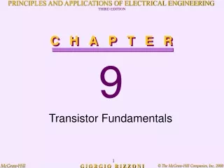
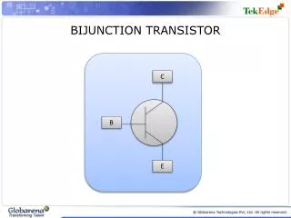
BIJUNCTION TRANSISTOR
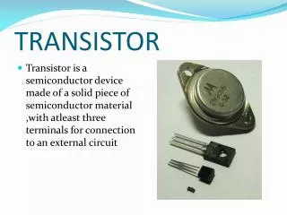
C. B. E. BIJUNCTION TRANSISTOR . Transistor . A transistor is a semiconductor device used to amplify and switch electronic signals. A transistor is made up of three layers – an ‘n’ layer sandwiched between two ‘p’ layers or a ‘p’ layer between two ‘n’ layers.

BIJUNCTION TRANSISTOR
E N D
Presentation Transcript
C B E BIJUNCTION TRANSISTOR
Transistor • A transistor is a semiconductor device used to amplify and switch electronic signals. • A transistor is made up of three layers – an ‘n’ layer sandwiched between two ‘p’ layers or a ‘p’ layer between two ‘n’ layers. • Doping of each layer is different and that is what is responsible for the operation(amplification).
The BJT – Bipolar Junction Transistor The Two Types of BJT Transistors: N P N P N P n p n p n p E C E C C C Cross Section Cross Section B B B B Schematic Symbol Schematic Symbol E E • Collector is moderately doped • Base is lightly doped • Emitter is heavily doped Click to view NPN Transistor Click to view PNP Transistor
BJT Relationships - Equations IE IC IE IC - VCE + + VEC - E C E C - - + + VBE VBC IB VEB VCB IB + + - - B B npn IE = IB + IC VCE = -VBC + VBE pnp IE = IB + IC VEC = VEB - VCB
DC and DC = Common-emitter current gain = Common-base current gain = IC = IC IB IE The relationships between the two parameters are: = = + 1 1 - Note: and are sometimes referred to as dc and dc because the relationships being dealt with in the BJT are DC.
Modes of Operation Active: • Most important mode of operation • Central to amplifier operation • Emitter –Base junction Forward biased and Collector –base Reverse Biased • Barrier potential of the junctions cancel each other out causing a virtual short • Ideal transistor behaves like an closed switch • Both junction are Forward biased Saturation: Cutoff: • Current reduced to zero • Ideal transistor behaves like an open switch • Both junction are Reverse biased
Three Types of BJT Configurations Biasing the transistor refers to applying voltage to get the transistor to achieve certain operating conditions. Common-Base Biasing (CB) input = VEB & IE output = VCB & IC Common-Emitter Biasing (CE) input = VBE & IB output = VCE & IC Common-Collector Biasing (CC) input = VBC & IB output = VEC & IE
BJT Transconductance Curve Typical NPN Transistor Collector Current: Transconductance: (slope of the curve) gm = IC / VBE IES = The reverse saturation current of the B-E Junction. VT = kT/q = 26 mV (@ T=300K) = the emission coefficient and is usually 1 IC 8 mA 6 mA 4 mA 2 mA VBE 0.7 V
Common-Base Circuit Diagram: NPNTransistor The Table Below lists assumptions that can be made for the attributes of the common-base biased circuit in the different regions of operation. Given for a Silicon NPN transistor.
Common-Base input characteristics • Input characteristics for the CB configuration gives relation between the input quantities, input voltage VEB and input current IE for fixed VCB values • The input circuit in CB configuration involves the emitter-base diode, which is forward biased in active region. Therefore, the relationship between VEB and IE is nothing but the forward characteristics of a diode
Common-Base input characteristics • In the above characteristics, VCB = Open represents the characteristics of the forward biased emitter • With increase of VCB, the curves shift downwards i.e., we get the same IE with less VEB. This is because, from the early effect increases the IE increases with VEB held constant
Common-Base out put characteristics Although the Common-Base configuration is not the most common biasing type, it is often helpful in the understanding of how the BJT works. Emitter-Current Curves
Circuit Diagram Common-Emitter Collector-Current Curves VCE IC IC + _ Active Region VCC IB IB VCE Saturation Region Cutoff Region IB = 0
Common Emitter Input Characteristics The input quantities for C.E. configuration are base current IB and base emitter voltage VBE The input characteristics curves are in between IB and VBE for various values of collector to emitter voltage VCE If VCE = 0 and if the base-emitter junction is forward biased, the input characteristics is the same as the characteristics of forward biased diode If VCE is increased then VCB increases By applying KVL around the transistor If VCE is increased then VCB increases
Common Emitter Input Characteristics Increase in VCB leads to decrease in effective base width WB| due to early effect, resulting in decrease of recombination and consequently, decrease in base current due to recombination.
Common Emitter output Characteristics • The output quantities in C.E. configuration are IC and VCE the o/p characteristics gives a relationship between IC and VCE with base current IB as a parameter. • This family of curves may be divided into three regions those are active region, saturation region and cutoff region.
Common-Collector • It is often called an emitter follower since its output is taken from the emitter resistor. • Is useful as an impedance matching device since its input impedance is much higher than its output impedance. • It is also termed a "buffer" for this reason and is used in digital circuits with basic gates.
Common-Collector Emitter-Current Curves • The Common-collector biasing circuit is basically equivalent to the common-emitter biased circuit except instead of looking at IC as a function of VCE and IB we are looking at IE. • Also, since 1, and • = IC/IE that means IC IE IE ActiveRegion IB VCE Saturation Region Cutoff Region IB = 0
Common collector input Characteristics Input Characteristics As VCB increases according to early effect base width decreases and IB decreases.
Common collector output Characteristics Output Characteristics: The common-collector circuit is basically same as the common-emitter, with the exception that the load resistor is in the emitter circuit, the output characteristics are similar to that of CE configuration. It is because
Transistor as amplifier • Transistor amplifies current as well as voltage and is a current operated device. • The CE configuration is widely used as it amplifies current and voltage unlike the other configurations. Click to view Image