Transistor Fundamentals for Amplifier Operation
210 likes | 268 Vues
Explore the controlled-source models and operation regions of a transistor, including simplified bias circuits and load-line analysis, for efficient amplifier design. Learn about BJT and MOSFET large-signal models, characteristics, and applications.

Transistor Fundamentals for Amplifier Operation
E N D
Presentation Transcript
9 Transistor Fundamentals
r o + + r v i _ in o in v i r r in in i i _ (a) Current-controlled current source (b) Voltage-controlled voltage source r o + + v i r _ in in o v r i r i in i in _ (c) Voltage-controlled current source (d) Current-controlled voltage source Figure 9.1 Controlled-source models of linear amplifier transistor operation
i 0 i 0 in in i i r r in i in i Current-controlled switch + + v 0 v 0 in in v r r v in i i in _ _ Voltage-controlled switch Figure 9.2 Models of ideal transistor switches
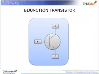
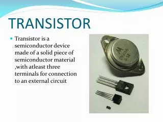
Collector Collector C C C C p n Base n B B Base p B B + + p n E E E E Emitter Circuit symbols Emitter Circuit symbols pnp transistor npn transistor Figure 9.4 Bipolar junction transistors
R C 1 k C R B B 40 k V 3 V CC V E BB V 12 V 1 R 4 V E V 2 500 Figure 9.10 Determination of the operation region of a BJT
By appropriate choice of I , R BB C and V , the desired Q point may CC be selected. I C C + R I C B B V CE + _ V I V BE CC BB _ E Figure 9.12 A simplified bias circuit for a BJT amplifier
50 m 45 m 40 m I = 250 A B 35 m I = 200 A Collector current, A 30 m B Q 25 m I = 150 A B 20 m I = 100 A 15 m B 10 m I = 50 A 5 m B 0 0 1 2 3 4 5 6 7 8 9 10 11 12 13 14 15 Collector-emitter voltage, V Figure 9.13 Load-line analysis of a simplified BJT amplifier
I + I C C C R + C I + I B B V + V CE CE + B R B – + V + V ~ _ BE BE V V B CC – E V BB Figure 9.15 Circuit illustrating the amplification effect in a BJT
I (mA) C 50 I 230 A = B 190 A 28.6 150 A Q 22 t 110 A 15.3 75 A 0 0 5 10 15 V (V) CE t Figure 9.16 Amplification of sinusoidal oscillations in a BJT
I C R R 1 C I + B V V CC + CE – V I BE E – R 2 R E Figure 9.20 Practical BJT self-bias DC circuit
I I C C + + I I R R R B B C C 1 V V CE + + CE R _ _ B V V BE _ BE _ V R V V V 2 CC I I CC R R CC BB E E E E (a) (b) Figure 9.21 DC self-bias circuit represented in equivalent-circuit form
C C I I I CEO C Cutoff state conditions: Active state conditions: B I = 0 B V = V V V BE BE B B I = 0 I 0 B B + – I = I I = I V C CEO C B V 0 V V CE CE E E C I C + I Saturated state conditions: V B sat – V = V BE B I 0 B + – I I V C B V = V CE sat E Figure 9.22 npn BJT large-signal model
Gate i D D Source Drain + n + n + p + V V _ DS DD + _ V G _ DD Bulk (substrate) S Figure 9.30(a) An n-channel MOSFET is normally off in the absence of an external electric field
i D D + + V V _ DS DD _ G + V _ + GS V S GG _ Figure 9.30(d) If the drain and gate supply voltages are both varied a family of curves (shown in Figure 9.31(b)) can be generated, illustrating the MOSFET cutoff, ohmic, saturation, and breakdown regions
(mA) i D = 2.8 V v 100 GS 80 2.6 V Q 60 2.4 V i D D 2.2 V 40 R + D G 2.0 V v DS + 20 – 1.8 V v V GS V GG – S ON 1.6 V 1.4 V 0 (V) 0 2 4 6 8 10 v DS Figure 9.32 n-channel enhancement MOSFET circuit and drain characteristic for Example 9.8
Gate Source Drain p Channel n p Figure 9.40(a) When the gate-source voltage is lower than -Vp, no current flows. This is the cutoff region
Gate Source Drain p n Channel p depletion regions Figure 9.40(b) For small values of drain-source voltage, depletion regions form around the gate sections. As the gate voltage is increased, the depletion regions widen, and the channel width (i.e., the resistance) is controlled by the gate-source voltage. This is the ohmic region of the JFET
Gate Source Drain p n Channel p Pinched-off channel Figure 9.40(c) As the drain-source voltage is increased, the depletion regions further widen near the drain end, eventually pinching off the channel. This corresponds to the saturation region
4 m 0 V 3 m – 0.5 V Drain Current, A 2 m – 1.0 V 2 m – 1.5 V 800 u – 2.0 V – 2.5 V V = – 3 V 0 GS 0 1.0 2.0 3.0 4.0 5.0 6.0 7.0 8.0 9.0 10.0 Drain-source voltage, V Figure 9.41 JFET characteristic curves