Download
1 / 2
20 likes | 230 Vues
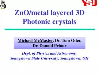
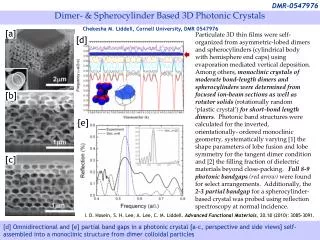
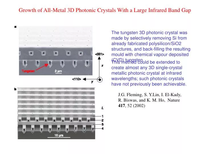
Growth of All-Metal 3D Photonic Crystals With a Large Infrared Band Gap. The tungsten 3D photonic crystal was made by selectively removing Si from already fabricated polysilicon/SiO2 structures, and back-filling the resulting mould with chemical vapour deposited (CVD) tungsten.

E N D
Growth of All-Metal 3D Photonic Crystals With a Large Infrared Band Gap The tungsten 3D photonic crystal was made by selectively removing Si from already fabricated polysilicon/SiO2 structures, and back-filling the resulting mould with chemical vapour deposited (CVD) tungsten. This method could be extended to create almost any 3D single-crystal metallic photonic crystal at infrared wavelengths; such photonic crystals have not previously been achievable. J.G. Fleming, S. Y.Lin, I. El-Kady, R. Biswas, and K. M. Ho, Nature 417, 52 (2002)
Mid-IR Metallic Layer-by-Layer Photonic Crystals Experimental Transmission, Reflection, and Absorption Spectra Unpolarized Incidence (001) Z Reflection Y Transmission Absorption Wavelength (m ) 4-Layer Tungsten Photonic Crystal a=4.2um, w=1.2um, h=1.5um J.G. Fleming et al., Nature 417, 52 (2002)