
Advancing Ion Electron Emission Microscopy at SIRAD Lab
Explore the cutting-edge IEEM technique developed at the SIRAD facility to study Single Event Effects (SEE) in electronic devices through high-precision ion impact position reconstruction and 3D imaging capabilities. Discover the innovative concept and design behind this advanced microscopy system.

Advancing Ion Electron Emission Microscopy at SIRAD Lab
E N D
Presentation Transcript
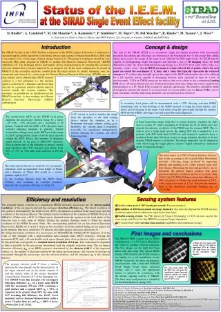
Status of the I.E.E.M. at the SIRAD Single Event Effect facility Introduction The SIRAD facility at the 15MV Tandem accelerator of the INFN Legnaro Laboratory is dedicated to characterising the global sensitivity of electronic devices and systems to Single Event Effects (SEE) due to ion impacts over a wide range of linear energy transfers [1]. The group is working to extend the very successful SEE study program at SIRAD to include Ion Electron Emission Microscopy (IEEM) capabilities [2]. The technique allows micrometric device characterisations by imaging the secondary electrons emitted from a surface impacted by an energetic ion. In the axial configuration developed at SIRAD [3], the secondary electrons, emitted from the target surface by axially impinging ions, are transported and focused by a microscope for Photon Electron Emission Microscopy (PEEM) onto an large annular micro-channel plate (MCP) detector Concept & design The aim of the SIRAD IEEM is to reconstruct single ion impact positions with micrometric precision. Resolution and efficiency are discussed in the bottom-left box of this poster. But, unlike others microscopes, the image of the target is not sufficient for SEE applications: the IEEM must be capable of distinguishing single ion impacts and perform a sort of 3D imaging where the third dimension is time. So, if in a standard microscope images is a 2D (X,Y) array filled with a value, e.g. intensity, counts, color..., for an IEEM an image is a time-ordered list of points, where for each point are stored the coordinates X, Y, time, and a value that typically represents the collected charge (c). To achieve this the light spot at the output of the MCP and phosphor has to be collected by a 2D sensitive device capable of discerning between spots separated in time by a few of microseconds; CCDs or CMOS arrays are too far too slow so we chose to use a commercial analog PSD [9] as a Position Sensitive Device. Dedicated readout electronics shapes the sensor signal before transferring it to a PC-based DAQ system for analysis and storage. An attractive alternative under development, intrinsically digital, is a system based on a beam splitter and twolinear CCDs, one for each coordinate. Another interesting alternative are novel pixel array detectors. coupled to a fast phosphor; i.e. the electron signal is converted to a luminous one that is then detected by a position sensitive photon detector located outside the vacuum chamber. The prototype, on standby for an installation on the SIRAD beam line, is now working in a Photon Electron Emission Microscopy (PEEM) configuration. A secondary focal plane will be instrumented with a CCD allowing real-time IEEM monitoring such as fine-focusing of the IEEM (instead of using the main sensor), and direct optical imaging of the target, back down along the optical path through the annular MCP and the PEEM, allowing a fast and repeatable target alignment. The double-stack MCP on the PEEM focal plane amplifies the microscope electron image by a factor ~106 with ~ 50% efficiency and a resolution of 16 lp/mm. Coupled with the MCP, a P47 phosphor layer converts outgoing electrons to photons. Typical acceleration voltages used in the MCP are in the range 1÷2 keV, giving photon yields of 40÷80 g/per electron exiting the MCP. Hence, the intensity of luminous signal depends on the gain of MCP+P47 sandwich. The relaxation time of the phosphor is short to ensure high repetition rates: P47 emission goes down, from 90% to 10%, in 55ns with peak emission at 400 nm [7]. A 45° mirror is used to transfer the image from the phosphor to the final sensing device outside the chamber, as in a Newtonian telescope scheme, adding great flexibility: the sensing chain is completely accessible for operational manipulations, without affecting the vacuum, and allows future upgrades. A final focal-plane image intensifier of 25mm diameter amplifies the light spot by a factor 103, with a resolution of 26 lp/mm [8], by far sufficient to not degrade the intrinsic resolution of the PEEM and the internal MCP. This is done to give a bright light spot to the analog PSD that is needed for it to perform well (S/N better than 1/1000 for each channel is needed to have a resolution better than 500 linear points on image diameter, the limit to do not degrade PEEM intrinsic resolution). The image intensifier can be dispensed with when using the single photon sensitive digital alternatives mentioned above (Concept & design). The main sensor is a PSD (Position Sensitive Device), that works according to the Lateral-Effect Photodiode principle, collecting charge produced by impacting photons and splitting it by a thin resistive layer into four charges. Measuring the four charges allows one to determine the photon impact position with great precision (intrinsic resolution proved to be better than 1/106). Our UV PSD [9] had a conversion efficiency of 68% e-h pairs/g at 400nm (the peak emission of P47), with a typical rise time of 1.5 ms, that puts the intrinsic limit to the theoretical maximum handling rate at ~3×10⁵ Hz. The main optical objective is made by two asymmetric achromats, with an equivalent focal length of 85mm and a diameter of 50mm: this results in a relative aperture equal to F1.7. At the working distance from the MCP (about 300mm), and assuming an isotropic phosphor emission, the acceptance efficiency is about 1%. Efficiency and resolution The principal figures of merit of a commercial PEEM electronic microscope are the lateral spatial resolution of the ion impact point and the ion impact detection efficiencyeion. The lateral resolution of the system is determined by the field of view (FOV), the intrinsic resolution of the microscope and the resolution of the electron detector. The intrinsic lateral resolution of the commercial PEEM [4] used at SIRAD is 250nm with a FOV of 250mm and is obtained when the aperture at the focal plane of the objective lens is wide open at 300mm. Closing the aperture diameter down to 50mm the lateral resolution of the PEEM becomes 50nm. The corresponding numbers for an Ion electron Emission Microscope (IEEM) are a factor 3 worse as the secondary electrons emitted during an ion impact are more energetic than those emitted by UV photons and suffer greater chromatic aberration [2]. By design the lateral resolution of a microscope for PEEM/IEEM (1000lines/FOV diameter) if of the order of that obtained with a high-resolution micro-channel plate (MCP) detectors. Viewing the maximum FOV with a 40 mm double-stack micro-channel plate electron detector with a resolution of 16 line-pairs/mm corresponds to a nominal lateral resolution of 0.4 mm. This value must be degraded as little as possible by the microscope (aberrations) and the complete detection chain. The ion impact detection efficiency eion of an IEEM system is determined by the electron yield Y of the impacted surface (i.e. the number of electrons emitted by the surface per ion impact), the fraction of electrons eT transmitted through the microscope onto the electron detector, and the efficiencyeD of the electron detector. Sensing system features Handles rates up to 5×10⁴ events per second (Poisson statistics). Resolution of 400 linear points on image diameter, that does not degrade the PEEM intrinsic resolution (equivalent resolution on target better than 1mm). Double sensing system: the PSD allows (X,Y,time) 3D-imaging; a CCD can watc exactly the same image and allows for fine IEEM focusing and target alignments. PC-based DAQ with real-time data analysis capabilities and continuous storage. First images and conclusions The SIRAD IEEM is under test in PEEM configuration, i.e. a UV source illuminates the target to produce electron emission. The two images on the right had been taken with this setup. The optical IEEM system, PSD detector and DAQ system is on standby for a test installation on the SIRAD beam line for basic performance measurements, with a dedicated SDRAM based Single Event Upset detection system, and to carry out operational studies to optimize the coexistence with the intense ongoing activity at SIRAD. The final axial configuration is scheduled for final installation in spring 2003. A 40mm step test copper grid viewed with a CCD with an equivalent FOV of 250mm. The light flares are caused by the non-planar target support. The average electron yield Y from a surface impacted by ions depends on the characteristics of the target material and on the atomic number Z and the surface value of the energy dependent Linear Energy Transfer LET of the impinging ion. For SIRAD beam line energies, the ion impact detection efficiency eion of a basic axial IEEM with the maximum 250 mm FOV, assuming a gold surface and a typical MCP eD = 55%, is expected to be greater than 50% for ions with Z>7 reaching full efficiency for Z>25. Novel materials such as B-doped diamond have yields a factor 2 higher than Au and eion = 100% is hence obtained for Z>15 [5][6]. The same image taken with the PSD. For each point the coordinates, impact time and collected charge are stored. This image is composed of about 5×10³ events. [1] J. Wyss, D. Bisello, D. Pantano et al. Nucl. Inst. And Meth. A 462 (2001) 426 [2] B. Doyle, G. Vizkelethy, D. S. Walsh, B. Senftinger, M. Mellon, Nucl. Inst. And Meth. B 158 (1999) 6 [3] D. Bisello et al. Nucl. Inst. And Meth. B 181 (1999) 6 [4] Staib Instrumente GmbH, Hagenaustrasse 22, 85416 Langenbach, Germany [5] A. Itoh, T. Majima, F. Obata, Y. Hamamoto, A. Yogo, Nucl. Inst. And Meth. B 193 (2002) 626 [6] D. Bisello et al. Secondary electron yield of metallic and doped diamond surfaces from ion impact in the 90-270 MeV energy range, ICNMTA 2002 contribution P2-13, corresponding author J. Wyss [7] El-Mul Technologies Ltd., Soreq, P.O. Box 571, 81104 Yavne, Israel, www.el-mul.co.il [8] Image Intensifier BV2582 BY-V 5N by Proxitronic, Robert-Bosch-Str. 34 D64625 Bensheim, www.proxitronic.de [9] UV PSD 2L20S by SiTek, BFI OPTILAS, www.bfioptilas.avnet.com


![Progressive Enhancement & Mobile [Funka 2012]](https://cdn4.slideserve.com/7565260/progressive-enhancement-mobile-dt.jpg)