Basic Electronic Assembly and Test
Basic Electronic Assembly and Test. Objectives Introduction to Discrete and IC level Packages Introduction to Substrates Mass Production Thru-Hole and SMT Assembly Processes Mass Production Test Strategies and Systems Introduction to PCB Layout

Basic Electronic Assembly and Test
E N D
Presentation Transcript
Basic Electronic Assembly and Test • Objectives • Introduction to Discrete and IC level Packages • Introduction to Substrates • Mass Production Thru-Hole and SMT Assembly Processes • Mass Production Test Strategies and Systems • Introduction to PCB Layout • Lab Exercise for PCB Layout to give you experience and confidence with an inexpensive PCB prototyping option
Basic Electronic Assembly and Test For Production Assembly Only Not for Prototype • Electronic Asm Team Deliverables: • Document in PPT slides all Product assembly levels and major assembly steps including boards, harnesses, package, etc. How will you assemble your product? • For each PCB Subassembly Document in PPT Slide Set: Dimensions, key component layout, type of substrate, BOM, mfg process diagram including solder processes (ID hand Ops), in-circuit tests, functional tests, ESS, as well as IPC assembly stds required. NOTE: If a PCB is a single design block, this is an individual deliverable
Basic Electronic Assembly and Test For Production Assembly Only Not for Prototype • Electronic Asm Individual Deliverables • Using the BOM Excel Template, for each design block, document a Mfg BOM. Document (cut/paste) into PPT slides. Also document where the block will reside in terms of the defined circuit boards (if applicable). Finally, document any special Mfg or Testing that will need to be done for this block.
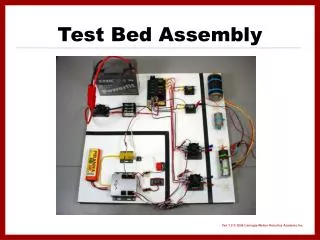
PCB Design Individual Lab Exercise • Using expresspcb.com Version 5.4.0 or Later • Download & Install Software from above link (first check to see if SW is already on PC) • Read Through Help Section – • Quickstart Tutorial for ExpressSCH • Quickstart Tutorial for ExpressPCB • Using ExpressSCH: Capture the Attached Schematic of Temp Sensor Circuit Using the Following Components • 3 ICs: LM35 SO8, OP07 Dip 8 • 6 Capacitors: Ceramic Monolithic Axial • 3 Resistors: 0.125W Axial
Using ExpressPCB: Create a Board Layout for the Temp Sensor Circuit Which Has the Following Characteristics • 1.5” x 2.2” • 2 Layer • Through Hole + 1 SMT Part • Placements as Shown for all parts • 25 mil power & ground traces, 10 mil signal traces • 56 mil power & ground input pads with silkscreen Labels • 56 mil output signal pads
Deliverables: • PCBExpress Schematic (.sch) electronic file • PCBExpress Layout (.pcb) electronic file • Powerpoint Slide Set of Schematic, Silkscreen, Top Side and Bottom Side Layers NOTE: To Copy from ExpressPCB and ExpressSCH, use the Print Scrn key from the keyboard, then when in Powerpoint or Word, use cntrl-V to paste the screen view.