Semiconductor Memory
Semiconductor Memory. Outline Memory Classification Memory Organization Memory Timing Parameters Memory Cores Periphery Reliability. Semiconductor Memory. What is Memories ? Circuits or systems that store digital information in large quantity Capacity

Semiconductor Memory
E N D
Presentation Transcript
Semiconductor Memory • Outline • Memory Classification • Memory Organization • Memory Timing Parameters • Memory Cores • Periphery • Reliability
Semiconductor Memory • What is Memories ? • Circuits or systems that store digital information in large quantity • Capacity • Circuit designers speak of memory capacity in terms of bits • System designer speak of memory capacity in terms of bytes( = 8 bits) • Large computer systems often state in terms of words ( = 32 or 128 bits) • Each byte or word is stored in a unique location called address Ex:1 Kb = 1024 bytes 64 Kb = 65536 bytes
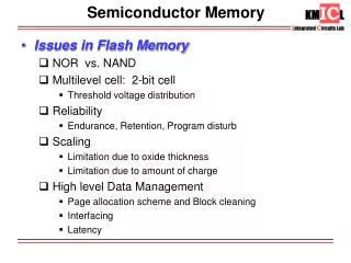
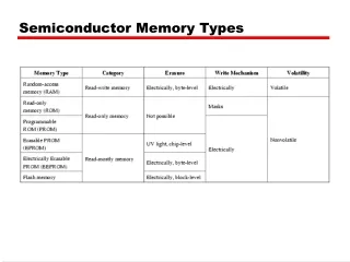
Semiconductor Memory Semiconductor Memory Classification Non-Volatile Read-WriteMemory Read-Write Memory Read-Only Memory Random Non-Random EPROM Mask-Programmed Access Access 2 E PROM Programmable (PROM) FLASH FIFO SRAM LIFO DRAM Shift Register CAM
Semiconductor Memory Timing Definitions • Read Access time: • Time it take to retrieve from the memory • Delay between read request and the moment the data available at the output • Write Access time • The time elapsed between a write request and the final writing of the input data into the memory • Cycle time • Minimum time requires between successive reads or writes
Semiconductor Memory Timing Definitions Source : Rabaey
Semiconductor Memory Array-Structured Memory Architecture Row address gives Word line to select row Amplifies swing to rail-to-rail amplitude Column address gives Bit line to select M-bit word Source : Rabaey
Semiconductor Memory Hierarchical Memory Architecture Source : Rabaey
Semiconductor Memory BL [0] BL [1] BL [2] BL [3] WL [0] V DD WL [1] WL [2] V DD WL [3] V bias Pull-down loads Read-Only Memory Cells: MOS OR Source : Rabaey
Semiconductor Memory V DD Pull-up devices WL [0] GND WL [1] WL [2] GND WL [3] BL [0] BL [1] BL [2] BL [3] Read-Only Memory Cells: MOS NOR Source : Rabaey
Semiconductor Memory V DD Pull-up devices BL [0] BL [1] BL [2] BL [3] WL [0] WL [1] WL [2] WL [3] Read-Only Memory Cells: MOS NAND All word lines high by default with exception of selected row Source : Rabaey
Semiconductor Memory V DD BL r word WL C bit c word Equivalent Transient Model • Word line parasitics • Wire capacitance and gate capacitance • Wire resistance (polysilicon) • Bit line parasitics • Resistance not dominant (metal) • Drain and Gate-Drain capacitance Model for NOR ROM Source : Rabaey
Semiconductor Memory Equivalent Transient Model • Word line parasitics • Wire capacitance and gate capacitance • Wire resistance (polysilicon) • Bit line parasitics • Resistance of cascaded transistors dominates • Drain/Source and complete gate capacitance V DD BL C L r bit c bit r word WL c word Model for NAND ROM Source : Rabaey
Semiconductor Memory Precharged MOS NOR ROM V f DD pre Precharge devices WL [0] GND WL [1] WL [2] GND WL [3] BL [0] BL [1] BL [2] BL [3] PMOS precharge device can be made as large as necessary, but clock driver becomes harder to design. Source : Rabaey
Semiconductor Memory • Disadvantages of ROM / PROM • ROM: Mask Programmable • Programming perform during manufacturing process • Involve the manufacturer • Unwelcome delay in product development • PROM: Fuse programmable • Customer to program memory one time • Single error in the programming process make the device unusable • Need multiple programmable device: NVRW: Nonvolatile Read-Write Memories
Semiconductor Memory • Nonvolatile Read-Write Memories • Virtually identical architecture to the ROM structure • Replace memory core with new device that permits its threshold voltage (Vt) to be altered electrically • Memory is programmed by selectively disable or enable some of these devices • To reprogram the programmed value must be erased first • The programming takes much longer than reading operation • Erasing mechanisms are different for each families.
Semiconductor Memory D G S • New Device: The Floating-Gate Transistor • Core of virtually every NVRW memory built today • Similar to MOS device except that an extra polysilicon strip called floating gate is inserted between the gate and channel Floating gate Control gate Source Drain t ox t ox + +_ n n p Substrate Device cross-section Schematic symbol Source : Rabaey
Semiconductor Memory • Effect of Floating Gate : Capacitive divider Source : Hodges
Semiconductor Memory • Example C1 = C2 = C
Semiconductor Memory • Operation • To turn on: Bias VG2 such that results in VG1 > VT* VG2 = 0 VG2 = VG1 = 0 VG1 = • Q:Given VT* = 2 V, how much VG2 have to be to turn on the device ?
Semiconductor Memory • Operation • To turn on: Bias VG2 such that results in VG1 > VT* VG2 = 0 VG2 = VG1 = -2 VG1 = • Q:Given VT* = 2 V, how much VG2 need to be to turn on the device ?
Semiconductor Memory • We can conclude the follows • Control gate voltage (VG2 ) that turns on the device can be altered depending on initial value of VG1 • If we have a way to change the initial value of VG1 we can effectively change the external VT of the device • More negative of VG1 results in more positive of external VT meaning the device is harder to turn on • How to change initial value of VG1 • One method to do this is using a mechanism called Hot Carrier Injection (HCI) or Channel Hot Electron injection (CHEI) for NMOS Device
Semiconductor Memory • HCI or CHEI • Gate and Drain is biased certain voltage(such as 5V), while Source and Substrate remain grounded so there is relative large Drain current flows. High field in Drain-Substrate depletion region results in an avalanche breakdown of the Drain-Substrate junction. • Field accelerates electrons to high velocity referred as Hot-Electrons. Fraction of them inject in to thin oxide and become trapped on the floating gate. As a result, it reduces internal node voltage until the vertical field is no longer sufficient to generate hot electrons thus it is self-limiting process. • Electrons can stay at the floating gate for a long period of time ( 10 years) Source : Hodges
Semiconductor Memory • Erasable Programmable ROM: EPROM • To program, using HCI to store charge (electrons) on floating gate resulting in a negative VG1. Thus increasing external VT so that VG2 can not turn on device. Once the device is disable it does not discharge the bit line. Therefore it is interpreted as store “1” • To Erase, Using strong ultraviolet light to assist removing of the stored charge (electrons). As a result, VG2 can turn on the device. Once the device is enable, it can discharge the bit line. Therefore it is interpreted as store “1”
Semiconductor Memory • EPROM Source : Hodges
Semiconductor Memory • Example: An EPROM with threshold voltage 1 V relative to Gate1 1) What is threshold voltage relative to Gate2 2) After programming, will this device turn on if VG2 = 5 V, if not what VG2 will turn it on ?
Semiconductor Memory EPROM • Advantages • Extremely simple and dense, 1T cell • Attractive for applications that do not require regular programming • Disadvantages • Off-system programming-labor intensive procedure • Write/Erase perform on the array. • HCI damages the device • High power consumption during programming
Semiconductor Memory • Electrical Erasable PROM: EEPROM • Using Floating gate Tunneling Oxide (FLOTOX) device as a storage device • FLOTOX is similar to FAMOS except it has two oxide thicknesses and occupies larger area • Using Fowler-Nordheim tunneling for both inject and remove charge from floating gate to change device VT. Thus it is a reversible process but not a self-limiting process. • Because its threshold voltage is difficult to control each cell requires additional MOS as a access (or selective) transistor resulting in 2T structure which needs larger area than EPROM
Semiconductor Memory • EEPROM I Gate Floating gate Drain Source V -10 V GD 20 – 30 nm 10 V 1 1 n n Substrate p 10 nm Fowler-Nordheim I-V characteristic FLOTOX transistor Source : Rabaey
Semiconductor Memory • EEPROM Operation • When apply voltage between Gate and Drain (VGD) so that it creates electric field exceed 107 V/cm across the thin oxide, electrons will start tunneling through the thin oxide • The current due to tunneling increases linearly with applied voltage. • Since the process is reversible, erase or program can be achieved by simply reversing the applied voltage.
Semiconductor Memory • EEPROM Write 0V Vdd 12V Float Reduce VT of FLOTOX Source : Hodges
Semiconductor Memory • EEPROM Erase 12V Vdd 0V Float Raise VT of FLOTOX Source : Hodges
Semiconductor Memory • EEPROM Read Vdd Vdd 0V If device turn on BL will be discharged = “L” Source : Hodges
Semiconductor Memory EEPROM • Advantages • On-system programming • FN tunneling damages devices slower than HCI • Write/Erase usually performs on bytes, although bit-by-bit access is possible • Disadvantages • FLOTOX is larger than FAMOS of EPROM • Highly susceptible to process variation particularly VT • Need an extra MOS for access • Limited number of write/erase cycle due to threshold shifting toward each other
Semiconductor Memory • NOR Flash • Combine the density of EPROM and versatility of EEPROM • NOR structure use HCI to program and use FN tunneling to erase • Erasure and programming times are slow due to need for precise control of the threshold • Erasure performs in bulk for a complete chip or sub-section of memory and takes between 100ms to 1 s • Perform VT checking during erasure and adjust erasure time dynamically • Fast random read access time thus suitable for program-code storage
Semiconductor Memory • NOR Flash Source : Hodges
Semiconductor Memory • NOR Flash –Write • Use HCI to program: source voltage is connected to GND, then Vd is applied to selected bitline while Vpp is applied to selected wordline Source : Hodges
Semiconductor Memory • NOR Flash –Erase • Use FN tunneling: Apply GND to all Gate (WL), high voltage of Vs to the source node • Transistors connected to source connections are all erased at the same time Source : Hodges
Semiconductor Memory • NOR Flash –Read • Apply GND to source connection, precharging the bitline to Vd and enable wordline with a Vread Source : Hodges
Semiconductor Memory • NAND Flash • 40% smaller and more dense than NOR array • Typically use FN tunneling for both write and erase which allows a much larger cycle limit usually more than 106 cycles • Fast write/erase and fast serial access but slower random access than NOR • Read operation is similar to NAND ROM • Suitable for applications that do not need fast random access such as video/audio file storage
Semiconductor Memory • NAND Flash • Wordlines are normally high but one will go low and active low when decoder is activated • Erase: BL and Source are high, WL is GND results in negative VT • Write “1”: SSL isolates source, then BL is GND and WL is high causing VT to increase • Write “0”: Keeping BL high so VT does not change • Read: SSL and DSL are enable. Then operate the same way as NAND ROM Source : Hodges