5.1 Semiconductor main memory
5.1 Semiconductor main memory. Organization The basic element of a semiconductor memory is the memory cell. Semiconductor memory cells properties: They exhibit two stable state to represent binary 1 and 0 They are capable of being written into at least once, to set the state.

5.1 Semiconductor main memory
E N D
Presentation Transcript
5.1 Semiconductor main memory • Organization • The basic element of a semiconductor memory is the memory cell. • Semiconductor memory cells properties: • They exhibit two stable state to represent binary 1 and 0 • They are capable of being written into at least once, to set the state. • They are capable to being read to sense the state.
The cell has three functional terminals capable of electrical signal: • The select terminal: it select a memory cell for a read or write operation. • The Control terminal: indicate read or write. • The other terminal are used for writing and reading - For writing: the other terminal provides an electrical signal that sets the state of the cell to 1 or 0 - For reading that terminal is used for output of the cell’s state.
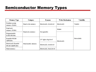
Semiconductor memory • RAM (Random Access Memory) • RAM characteristic: - Read/Write - Volatile - Temporary storage - Static RAM (SRAM) or dynamic RAM (DRAM)
DRAM (Dynamic RAM) • Bits stored as charge in capacitors the presence or absence of charge in the capacitor is interpreted as a binary 1 or 0 • Require periodic charge refreshing to maintain data storage. • Charges leak away, even with power continuously applied. • Smaller per bit, Slower • Less expensive • Need refresh circuits • Essentially analogue • Level of charge determines value
DRAM Structures • The address line is activated when the bit value from this cell is to be read or written. • The transistor acts as a switch that is closed if a voltage is applied to the address line and open other wise. • For write operation: • A voltage signal is applied to the bit line; high voltage represent 1 and low voltage represent 0 • A signal is then applied to the address line allowing the charge to be transfer to the capacitor.
DRAM Structures • For read operation: • The address line is selected, • Then transistor turns on • Charge stored on the capacitor to fed out onto a bit line and to the sense amplifier • Amplifier compares the capacitor voltage to a reference value if its 1 or 0 • The readout from the cell discharges the capacitor, which must be restored to complete the operation.
Static RAM (SRAM) • It is a digital device that uses the same logic element in the processor, bits stored as on/off switches • No charges to leak • No refreshing needed when powered • More complex construction • Larger per bit • More expensive • Does not need refresh circuits • Faster • Cache • Uses flip-flops
DRAM versus SRAM • Both volatile • Power needed to preserve data • Dynamic RAM - Simpler to build, smaller - More dense ( more cells per unit area) - Less expensive - Needs refresh circuitry - Larger memory units • • Static RAM - Faster - Used for Cache memory
ROM (Read Only Memory) • Permanent storage of data that cannot be changed • Nonvolatile; no power source is required to maintain the bit values in memory. • It is possible to read a ROM. • Important application of ROMs - Microprogramming (see later) - Library subroutines - Systems programs (BIOS) - Function tables
Types of ROM - Written during manufacture - Very expensive for small runs • Programmable ROM (PROM) (once) - The writing process is perform electrically and may be perform by a supplier or customer. - Special equipment is require for the writing or “Programming” process. - Read “mostly”
Types of ROM • Erasable Programmable (EPROM) - Is read and written electrically - Can be altered multiple times - More expensive than PROM. • Electrically Erasable (EEPROM) - Takes much longer to write than read - Flexibility of being updatable in place, using ordinary bus control, address, and data lines. - Is more expensive than EPROM - Support fewer bits per chip.
Types of ROM • Flash memory - Erase whole memory electrically. - Much faster than EPROM - It is possible to erase just blocks of memory - It uses only on transistor per bit
Organization in detail • A 16Mbit chip can be organized as 1M of • 16 bit words • A bit per chip system has 16 lots of 1Mbit • chip with bit 1 of each word in chip 1 and • so on • A 16Mbit chip can be organized as a 2048 • x 2048 x 4bit array • Reduces number of address pins • Multiplex row address and column address • 11 pins to address (211=2048) • Adding one more pin doubles range of values so x4 capacity
Refresh operation • Refresh circuit included on chip • Disable the DRAM chip while all data cell are refreshed. • Refreshing Count step through all row values • Data are read out & written back into the same location. • Takes time • Slows down apparent performance
Chip Packaging • An integrated circuit is mounted on a package that contains pins for connection to the outside world. • Fig. 5.4 a shows an example EPROM package, which is an 8-Mbit chip organized as 1Mx8 . • The pins support the following signal lines: - The address of the word being access pins (A0-A19) - The data to be read out, 8 lines (D0-D7). - The power supply to the chip (Vcc) - A ground pin (Vss) - A chip enable (CE) pin - A program voltage (Vpp) that is supplied during programming Fig 5.4.b For 16-Mbit chip organize as 4Mx4
Module Organization • The number of chip is equal to the number bit per word • Fig. 5.5 shows how a memory module consisting of 256K-8bit words, an 18-bit address is needed and supplied to the module from external source. • Fig.5.6 shows the possible organization of memory consisting of 1M word by 8bits per word. We have four columns of chips each column containing 256Kwords arranged as in Fig.5.5
Interleaved Memory • Collection of DRAM chips • Grouped into memory bank • Banks independently service read or write • requests • K banks can service k requests simultaneously. • Increasing memory read or write rate by a factor of k
Error correction • Hard failure: Is a permanent physical defect so that the memory cells can not store data but become stuck at 0 or 1 or switch between 0 and 1. It can be detected by manufacturing. • Soft error: Is a random, nondestructive event that alters the content of one or more memory cells without damaging the memory. It can be caused by power supply problems. • Detected using Hamming error correcting code.
Error-Correcting Code Function Fig.(5.7) • When an M-bit word of data is to be stored and the code is of length k bits, then the actual size of the stored word is M + K bits, when it read out the code is used to detect and possibly correct errors. A new set of k code bits is generated from the M data bits and compared with the fetched code bits. The comparison yields one of three results: 1. No error are detected. The fetch data bits are sent out. 2. An error is detected, and it is possible to correct the error. The data bits plus error correction bits are fed into the corrector, which produces a corrected set of M bits to be sent out. 3. An error is detected, but it is not possible to correct it. This condition is reported.
5.3 Advanced DRAM organization • There are many enhancements to the basic DRAM architecture have been explored. • In this section we discus this types: • Synchronous DRAM (SDRAM) The SDRAM exchanges data with the processor synchronized to an external clock signal and running at the full speed of the processor/memory bus without imposing wait stats. With synchronous access, the DRAM moves data in and out under control of the system clock.
Synchronous DRAM (SDRAM) • Access is synchronized with an external clock • Address is presented to RAM • RAM finds data (CPU waits in conventional DRAM) • Since SDRAM moves data in time with system clock, CPU knows when data will be ready • CPU does not have to wait, it can do something else • Burst mode allows SDRAM to set up stream of data and fire it out in block • DDR-SDRAM sends data twice per clock cycle (leading & trailing edge)
Rambus DRAM • Adopted by Intel for Pentium & Itanium processors • It has become the main competitor to SDRAM • It has a vertical packages with all pins on one side • Data exchange over 28 wires < cm long • Bus addresses up to 320 RDRAM chips and rated at 1.6Gbps • It delivers address and control information using asynchronous block protocol • After an initial 480ns access time. This produces the 1.6 GBps data rate.
Double-Data-Rate SDRAM(DDR SDRAM) • SDRAM can only send data once per clock • Double-data-rate SDRAM can send data • twice per clock cycle • Rising edge of the clock pulse and falling edge. • Fig.5.15 shows the basic timing for the DDR read
Cache DRAM • It developed by Mitsubishi. • Integrates small SRAM cache (16 kb) onto generic DRAM chip • Used as true cache - 64-bit lines - Effective for ordinary random access • To support serial access of block of data - refresh bit-mapped screen - CDRAM can prefetch data from DRAM into SRAM buffer - Subsequent accesses solely to SRAM