Download
1 / 35
450 likes | 864 Vues
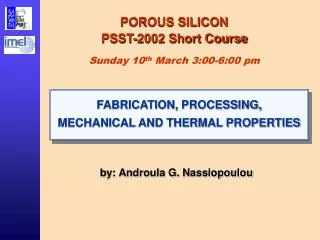
POROUS SILICON PSST-2002 Short Course Sunday 10 th March 3:00-6:00 pm. FABRICATION, PROCESSING, MECHANICAL AND THERMAL PROPERTIES. by: Androula G. Nassiopoulou. IMEL,/NCSR Demokritos, PSST 2002, Tenerife. POROUS SILICON FORMATION BY ELECTROCHEMICAL DISSOLUTION OF SILICON (II).

E N D
POROUS SILICON PSST-2002 Short Course Sunday 10th March 3:00-6:00 pm FABRICATION, PROCESSING, MECHANICAL AND THERMAL PROPERTIES by: Androula G. Nassiopoulou
IMEL,/NCSR Demokritos, PSST 2002, Tenerife POROUS SILICON FORMATION BY ELECTROCHEMICAL DISSOLUTION OF SILICON (II) Cross sectional view of a conventional double-tank cell (2)
IMEL,/NCSR Demokritos, PSST 2002, Tenerife EFFECT OF ILLUMINATION IN POROUS SILICON FORMATION IN HF-WATER OR ETHANOLIC SOLUTIONS For a review, see : Α. Halimaoui in: Properties of porous silicon, edited by: L.T.Canhan EMIS DATAREVIEWS series No 18 IEE 1997 Anodization of p-type silicon: in HF-water or ethanolic solutions Anodization of n-type silicon: in above solutions: need for illumination Effect of illumination: electron/hole pair generation holes are involved in the chemical reactions for silicon dissolution For a doping level < ~1018cm-3 :Silicon dissolution occurs in the dark only at high voltage (>5V) Under illumination: porous silicon formation occurs at lower potentials (<1V) (surface layer: nanoporous, underlying layer: macroporous) For a doping level >1018cm-3 : porous silicon formation mesoporous even in the dark (holes generated by electric field induced avalanch breakthrough Using specially “designed” electrolytes: macroporous silicon formation on n-type silicon without any illumination is possible (current bursts model) Ref: H.Föll et al., Physica Status Solidi (1) 182,7 (2000) (3)
IMEL,/NCSR Demokritos, PSST 2002, Tenerife STAIN ETCH POROUS SILICON FILM GROWTH References: •G.Di Francia et al, J.Appl. Phys. Vol 77 (1995) p 3549 • Di Francia, Solid State Communications, vol 96 (1995) 79 • Noguchi et al., Appl. Phys. Lett. 62(12) 1993, 1429 Obtained films : • In general non-uniform (due to random anodic and cathodic sites) • With Al-150 to 200 nm thick on Si instantaneous reaction of silicon with HF/HNO2/H2O etchant, due to the reaction of Al and HNO3 to provide holes (selective formation) of PS) • Use of sonication during stain etching: • thicker PS films • more rough PS surface • Simple illumination of Si in 50% HF with HeNe laser: porous silicon formation • Si dissolution without electric field • Chemical solution: HF/nitricacid/ water Key component:hole (h+) generation cathode: HNO3+3H+NO+2H20+3h+ anode : nh++Si+2H2OSiO2+4H++(4-n)e- SiO2+6HFH2SiF6+2H2O Above reaction: catalysed by HNO2 “incubation” period Influence of substrate doping It influences the incubation time • · p-type silicon: incubation time increases with substrate resistivity • n-type silicon: “ “ decreased with increasing resistivity (4)
Type I multilayers: Fabrication: IMEL/ NCSR Demokritos, PSST 2002, Tenerife MULTILAYER STRUCTURES OF POROUS SILICON (I) Based on the following properties: • Porosity depends on anodization current density • Porosity depends on illumination parameters in n-type silicon • Porosity depends strongly on doping concentration • The silicon skeleton in the already etched structures is not affected during further processing (hole depleted) The porosity in the layers is monitored by changing: • The anodization current density • The illumination parameters in n-doped substrates Ref: M. Thönissen and M.G.Burger in: Properties of porous silicon, edited by L.T.Canham, EMIS Datareviews Series No 18 IEE, 1997 (5)
Gas flow T1 T2 T1 T2 Gasflow IMEL,/NCSR Demokritos, PSST 2002, Tenerife PRINCIPLE OF OPERATION OF THE GAS FLOW SENSOR T1 = T2 T1 < T2 (6)
Cross sectional view of a conventional single-tank cell Cross sectional view of a lateral anodization cell IMEL/NCSR Demokritos, PSST 2002, Tenerife POROUS SILICON FORMATION BY ELECTROCHEMICAL DISSOLUTION OF SILICON (I) Electrochemical solution: HF-based DIFFERENT ANODISATION CELLS (7)
Interface sharpness: IMEL/NCSR Demokritos, PSST 2002, Tenerife MULTILAYER STRUCTURES OF POROUS SILICON (II) Type II multilayers: The layered structure is defined before anodization (alternate layers with differentdoping concentration) • In type-I multilayers given by the transition of the anodization current and its effect on etching.Transition zone below 15 nm is achieved. • In type-II multilayers given by the epitaxy (8)
IMEL/NCSR Demokritos, PSST 2002, Tenerife APPLICATIONS OF MULTILAYER PS STRUCTURES • Interference Filters • Waveguides • Porous silicon mirrors for biological applications (9)
IMEL/NCSR Demokritos, PSST 2002, Tenerife MULTILAYER STRUCTURES OF POROUS SILICON (III) • Type-Imultilayers by varying anodisation current • Current density: 6 and 104 mA/cm2 • Etching time: 4.83 and 1.33 sec • Type-I multilayers by varying the illumination density • Current density: 6.4 mA/cm2 • Type-II multilayers on epitaxially grown silicon layers with varied doping concentration of 1017 and 1019 cm-3 (a) (b) (c) Ref: M. Thönissen and M.G.Burger in: Properties of porous silicon, edited by L.T.Canham, EMIS Datareviews Series No 18 IEE, 1997 (10)
DERIVATIZED POROUS SILICON MULTILAYERS AND BIOLOGICAL MIRRORS (11) Ref: L.T. Canham et al, Phys. Stat. Sol. (a) 182, 521 (2000)
Cracking: • due to capillary stresses associated with the nanometric size of the pores • occurs for PS layers thicker than a critical thickness hc (hc depends on the porosity and on the surface tension of the drying liquid) IMEL/NCSR Demokritos, PSST 2002, Tenerife DRYING OF POROUS SILICON (I) Crucial in order to avoid cracking Example : Ref. D.Bellet in: Properties of Porous silicon (12)
IMEL/NCSR Demokritos, PSST 2002, Tenerife DRYING OF POROUS SILICON (II) Origin of cracking : evaporation of the pore liquid gives rise tocapillary tension Maximum capillary stress : at the critical point when the menisci enter the pores Induced pressure: ΔΡ =2γLV/r, γLV =surface tension, r = pore radius Example: For water γLV = 72mJ/m2 for r = 5nm ΔΡ = 30ΜPa (300 bar) Capillary pressure: not hydrostatic, since normal air drying is out of equilibrium Measurement of induced tensile stresses: By measuring wafer curvature Using X-ray diffraction (measuring lattice parameters) (13)
IMEL/NCSR Demokritos, PSST 2002, Tenerife DRYING OF POROUS SILICON (III) Drying techniques to avoid cracking • Water or pentane drying (pentane:lower surface tension than water) • Supercritical drying • Most efficient drying method (L.T. Canham et al. Nature (UK) Vol 368 (1994) p133) • Used fluid: CO2, drying: above the critical point (40oC, 163 bar) • Result: ultrahigh porosity films • Freeze drying • The fluid inside the pores is frozen and then sublimed under vacuum (no interfacial tension) (14)
(15) Ref: M. Thönissen and M.G.Burger in: Properties of porous silicon
IMEL/NCSR Demokritos, PSST 2002, Tenerife AGEING OF POROUS SILICON It results from the reaction of the material with its environment Intentionally oxidize PS Isolate the internal surface by capping Modify the internal surface In order to minimize storage effects: Impregnate the pores (16)
a)Epitaxially deposited capping layers • CoSi2 and SiGe, deposited at 600oC stabilization of strain (Kim et al., J. Appl. Phys, 69 (1991) 2201) • Si on porous silicon. Fabrication of SOI or bond-and-etchback SOI (BESOI) • GaAs on PS: for monolithic integration of optoelectronics with Si ICs • Diamond for high temperature electronics • PbTe, for mid-infrared (3-5 μm) optoelectronic devices IMEL/NCSR Demokritos, PSST 2002, Tenerife CAPPING OF POROUS SILICON I Used to avoid ageing (17)
IMEL/NCSR Demokritos, PSST 2002, Tenerife CAPPING OF POROUS SILICON II • Organic/polymeric capping layers • Paraffin on the surface of PS (Tischler et al). Short term stabilization of PL • Capping with conducting polymers, as plyaniline, polypyrrole • Polymer within the pores • Metallic capping layers • Ti or Co silicides • Al deposition – protection in ambient air • Reduces C and O pick-up, retains F • Al capping – Protection during analysis • avoids oxidation and carbonization of samples, and H or F desorption • Dielectric capping • CVD deposited SiO2 on medium porosity Si minimizes ion-beam induced ageing • Ion-implanted O or N, or PECVD-deposited SiO2, Si3N4 • No result on PL stabilization (18)
SURFACE MODIFICATION OF POROUS SILICON Surface of freshly etched porous silicon: hydrogen-passivated (SiH, SiH2, SiH3) good electronic passivation Surface modification : limited stability • Oxidation • Anodic, chemical, thermal • Nitridation • Rapid thermal annealing in N2 or NH3 • Organic chemical derivatisation • Stabilisation by organic groups, process stopped at a monolayer • Surface covered with SiH and SiCH2CH3 upon dissociative adsorption • of diethylsilace (Dillon et al. (1992) • Grafting of trimethylsiloxy groups. Substitution of - H with - OSi (CH3)3 • Anderson et al 1993) • Thermal derivatisation with alcohols (Hory et al. 1995, Kim et al. 1997) • Grafting of alkoxy groups (Li et al. 1994) • Electrochemical derivatisation Ref: J.N. Chazalviel et al in: Properties of Porous silicon (19)
STABILIZATION AND FUNCTIONALIZATION VIA HYDROSILYLATION AND ELECTROGRAFTING REACTIONS Substitution of the silicon hydride bonds with silicon carbon bonds • LAM (Lewis acid mediated) reaction (hydrosilylation) • Light-promoted hydrosilylation • Cathodic electrografting Ref: J.M. Buriak, Adv. Mat. 11, 265 (1999) (21)
IMEL/NCSR Demokritos, PSST 2002, Tenerife ELASTIC PROPERTIES OF PS They differ drastically from those of bulk silicon X-ray diffraction Young’s modulus of P.S Microechography and measurement of acoustic signature (measuring reflection and transmission parameters versus frequency) Measured by Nanoindentation investigation (Nanoindenter: it measures force and displacement as an indentation is performed on the material using a very low load) Brillouin scattering used to investigate the surface acoustic waves on a PS-layer General tendency: PS is less stiff than bulk silicon (with lower Young’s modulus values) (22)
YOUNG’S MODULUS VALUES OF POROUS SILICON Ref: M. Thönissen and M.G.Burger in: Properties of porous silicon, edited by L.T.Canham, EMIS Datareviews Series No 18 IEE, 1997 (23)
THERMAL CONDUCTIVITY OF POROUS SILICON Very different from that of bulk silicon Bulk silicon : 145 W m-1K-1 Porous silicon : depends on porosity [1,2] [1,2] 40 A. Drost et al. Sens. Mat. (Japan), vol 7 (1995) p 111 W.Lang et al. Mater. Res. Soc. Symp. Proc. (USA) vol. 358 (1995) p561 A.G.Nassiopoulou et al. Phys. St. Sol. (a) 182, 307 (2000) (24)
Resistor on bulk silicon Temperature distribution around a heater on bulk silicon Ref: A.G. Nassiopoulou and G. Kaltsas, Phys. Stat. Solidi (9) 182, 307 (2000). (25)
Resistor on PS Temperature distribution around a heater on porous silicon Temperature distribution around a heater on a free standing silicon membrane Resistor on a free standing silicon membrane (26) Ref: A.G. Nassiopoulou and G. Kaltsas, Phys. Stat. Solidi (9) 182, 307 (2000).
IMEL/ NCSR Demokritos, PSST 2002, Tenerife LOCAL FORMATION AND PATTERNING OF POROUS SILICON Necessary in applications using monolithic integration of the corresponding devices and structures on the silicon substrate LITHOGRAPHIC PATTERNING Most commonly used masking materials: • Photo resists: • Common photoresists (AZ5214): withstand etching solutions only for short anodization time. • Use of SU8 photoresist: long anodization time (V.V. Starkov et al (this Conference)) • Silicon dioxide: For anodization times of a few minutes • Stoichiometric silicon nitride or silicon carbide: Resistant to the anodization solution but they show problems related to stress effects and cracking • Non-stroichiometric nitride, deposited by LPCVD good mask • Double layer of polysilicon/SiO2 Perfect mask for porous silicon micromachining. (27)
IMEL/ NCSR Demokritos, PSST 2002, Tenerife Examples of local anodization through a lithographic mask Silicon nitride mask Ref:Α.Nassiopoulou et al Thin Solid Films 255 (1995) 329 SiO2 mask:anodization time: 1 min Ref:Α.Nassiopoulou et al. Thin Solid Films 255 (1995) 329 Polysilicon mask Ref: G.Kaltsas and A.G.Nassiopoulou, Sensors and Actuators A65(1998) 175 (28)
IMEL/NCSR Demokritos, PSST 2002, Tenerife IMEL, NCSR Demokritos, PSST 2002, Tenerife LITHOGRAPHIC PATTERNING USING POLY/SiO2 MASK APPLICATION IN MICROMACHINING Reference: G.Kaltsas and A.G.Nassiopoulou, Sensors and Actuators A65 (1998) 175 (29)
Examples of free standing polysilicon membranes and cantilevers. POROUS SILICON MICROMACHINING Use of porous silicon as sacrificial layer for the formation of free standing membranes on top of a cavity Ref: G. Kaltsas and A.G. Nassiopoulou, Sensors and Actuators, A65 (1998) 175-179. (30)
DRY ETCHING OF POROUS SILICON • As prepared PS layers are etched • 6-7 times faster compared to Si. • Typical etch rates for SF6: • RIE : 6.8 μm/min (Si:1.5μm/min) • HDP :66 μm/min (Si:10 μm/min) • Etching rate depends on: • The porosity • Aging of the layer. • Thermal treatment. • The etch rate of thermally treated PS layersis significantly smaller than that of freshly etched PS. • HDP :0.33 μm/min Ref: A. Tserepi et al, PSST 2002, abstract book page 187. (31)
100μm IMEL,/NCSR Demokritos, PSST 2002, Tenerife SUSPENDED POROUS SILICON MICRO-HOTPLATES FOR GAS SENSORS High temperatures (>400oC) can be obtained with very low energy consumption (<30mW) Ref: C. Tsamis and A.G. Nassiopoulou, unpublished results. (32)
P=42mW P=46.6mW P=50mW P=57mW Suspended Porous Silicon membranes with Pt heater (60x60μm2) (33) Ref: C. Tsamis and A.G. Nassiopoulou, unpublished results.
IMEL,/NCSR Demokritos, PSST 2002, Tenerife EXAMPLE: GAS FLOW SENSOR Ref: G. Kaltsas and A.G. Nassiopoulou, Sensors and Actuators 76 (1999) 133-138. (34)
Sensor characteristics (35) Ref: G. Kaltsas and A.G. Nassiopoulou, unpublished results