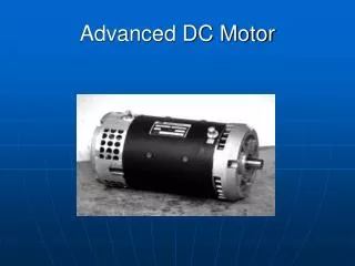
DC MOTOR
DC MOTOR. DC MOTOR WORKING. H BRIDGE DC MOTOR. INTERFACING WITH DC MOTOR. OPERATION:. TRANSLATE ELECTRIC ENERGY MECHANICAL MOVEMENT + TO – LEADS PRODUCE THE MOTOR CLOCKWISE REVERSE POLARITY MOTOR REVERSES LOAD VOLTAGE SPEED IS REPRESENTED BY RPM.

DC MOTOR
E N D
Presentation Transcript
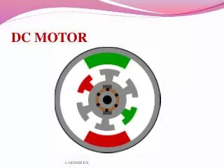
DC MOTOR LAKSHMI.B.E.
DC MOTOR WORKING LAKSHMI.B.E.
H BRIDGE DC MOTOR LAKSHMI.B.E.
INTERFACING WITH DC MOTOR LAKSHMI.B.E.
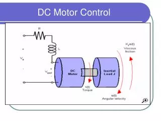
OPERATION: • TRANSLATE ELECTRIC ENERGYMECHANICAL MOVEMENT • + TO – LEADS PRODUCE THE MOTOR CLOCKWISE • REVERSE POLARITY MOTOR REVERSES • LOAD VOLTAGE • SPEED IS REPRESENTED BY RPM LAKSHMI.B.E.
USING L293,RUN A DC MOTOR, SWITCH P2.0 IF SW=0,ROTATE CLOCK,SW=1 , ROT ANTICLOCK • ORG 0H • MAIN: • SETB P1.0 ; ENABLE • JNB P2.0 ,CLOCK ;CHECK THE CLOCK • CLR P1.1;INPUT 1 ;COUNTER CLOCKWISE • SETB P1.2;INPUT2 ; • CLOCK: • SETB P1.1;INPUT 1 ; CLOCKWISE • CLR P1.2;INPUT2 • SJMP MAIN • END LAKSHMI.B.E.
DS12887 INTERFACING WITH 8051 LAKSHMI.B.E.
DS 12887: LAKSHMI.B.E.
DS 12887: LAKSHMI.B.E.
DS 12887: LAKSHMI.B.E.
PIN DIAGRAM FOR DS 12887 LAKSHMI.B.E.
Memory: • 128 bytes of non volatile ram • 14 bytes of RAM ,for clock ,calender and control register • 114 bytes of NV-RAM LAKSHMI.B.E.
AS:ADDRESS STROBE is an input pin,on the falling edge it will cause the address to be latched MOT: DS: • MOT is connected to ground • MOT=GND • DATA STROBE • DS=READ • DS is connected to RD of 8051 LAKSHMI.B.E.
R/W:input pin .MOT=GNDWrite signal CS: IRQ: • Active low signal • To access read and write • It only access external vge>4.25v • Output pin • Active low pin • It is in “B”register LAKSHMI.B.E.
SQW: RESET: • Output pin .it produce 15 different square wave • Pin 18 is reset.It is an input. • Active low pin LAKSHMI.B.E.
Setting the time(16:15:50 pm) MOV R0,#10;ADDR OR ’A’ REGISTER MOV A,#20H; D6-D4 010 OSC MOVX @R0,A;SEND IT TO REG MOV R0,#11; REG B MOV A,#83H; BCD 24 HRS,DAYLIGHT MOV X @R0,A • MOV R0,#0; SECONDS AT ADDR 0 • MOV A,#50H;SECONDS=50 • MOVX @R0,A; SET SECONDS • MOV R0,#02; • MOV R0,#15H; • MOVX @R0,A; • MOV R0,#04; • MOV R0,#16H • MOVX @R0,A; LAKSHMI.B.E.
Interfacing external memory LAKSHMI.B.E.
ROM • Non-volatile Data • Mask ROM • Data written during chip fabrication • PROM • Fuse ROM: Non-rewritable • EPROM: Erase data by UV rays • EEPROM: Erase and write through electrical means • Speed 2-3 times slower than RAM • Upper limit on write operations • Flash Memory – High density, Low Cost LAKSHMI.B.E.
ROM: LAKSHMI.B.E.
RAM • Random write and read operation for any cell • Volatile data • Most of computer memory • DRAM • Low Cost • High Density • Medium Speed • SRAM • High Speed • Ease of use • Medium Cost LAKSHMI.B.E.
RAM: LAKSHMI.B.E.
ADC and DAC INTERFACING LAKSHMI.B.E.
ADC : • ADC is widely used for data acquisition • Digital computers are digital but physical world is analog(continuous) • TRANSDUCER: • Physical quantity is converted to electrical quantity • Ex: load cell, strain gauge • To translate this analog to digital converter is used. LAKSHMI.B.E.
Step size: • The smallest change that can discerned by adc. • Conversion time: • The time takes to convert analog to digital LAKSHMI.B.E.
CS:Active low input RD: WR:START CONVERSION) • Input signal • Active low signal • Analogdigital • When CS=0 • is applied to RD pin • RDOE • Active low signal • Analogdigital • When CS=0 • is applied to WR pin LAKSHMI.B.E.
CLK IN CLK R • Input signal • External clock is used for timing • For internal clock generator CLK IN and CLK R are connected together to a capacitor and resistor LAKSHMI.B.E.
Vcc:+5v power supply Vin(+) and Vin(-): INTR: • They are differential anlog inputs Vin=Vin(+) -Vin(-) • Output pin • Active low • It is normally high,When conversion is finished ,it goes to low to CPU LAKSHMI.B.E.
D0 to D7:DIGITAL DATA OUTPUTPARALLEL ADC.Dout= Vin step size LAKSHMI.B.E.
RD BIT P3.7WR BIT P3.6INTR BIT P3.2;END OF CONVERSION;DISPLAYMOV P1,#0FFHSETB INTRAGAIN:CLR WRSETB WRHERE:JB INTR ,HERECLR RDMOV P1,#55HSETB RDSJMP AGAIN LAKSHMI.B.E.
DAC INTERFACING LAKSHMI.B.E.