Download
1 / 26
260 likes | 284 Vues
Explore the development of FPGA-based fixed-latency serial links for SuperB DAQ/Trigger systems, focusing on Xilinx FPGA transceivers and GTP architecture to achieve high-speed data transfers. Learn about clocking schemes and proof of concept testing for future applications.

E N D
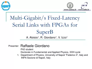
Multi-Gigabit/s Fixed-Latency Serial Links with FPGAs for SuperB A. Aloisio1, R. Giordano1, V. Izzo1 Raffaele Giordano Presenter: PhD student Doctorate in Fundamental and Applied Physics, XXIII cycle • Department of Physics, University of Napoli “Federico II”, Italy and • INFN Sezione di Napoli, Italy
Outline • Introduction • SuperB DAQ/Trigger architecture • GBT project at CERN • High-Speed FPGA transceivers • A FPGA-based link with fixed latency • Test on a custom backplane • Future work • Conclusion Raffaele Giordano - SuperB Computing Workshop - December 2008
Introduction • SuperB DAQ implementation requires fixed-latency serial links • The GBT Project at CERN suggests the deployment of FPGAs on the off-detector end of the link • In Naples: Development of a fixed latency serial link based on FPGA transceivers for DAQ/Trigger applications • Proof of concept: development of a compatible replacement for an obsolete SerDes chip-set (G-Link) deployed in the ATLAS experiment • Test of FPGA-embedded SerDes for local data transfers on a custom backplane Raffaele Giordano - SuperB Computing Workshop - December 2008
From : Dominique Breton SuperB meeting – La Biodola – June 2008 FCTS: Fast Control and Trigger System FEC: Front End Cards ROM: Read Out Module Raffaele Giordano - SuperB Computing Workshop - December 2008
From : Dominique Breton SuperB meeting – La Biodola – June 2008 Raffaele Giordano - SuperB Computing Workshop - December 2008
From : Paulo Moreira – NSS08 Conference – Dresden – October 2008 Raffaele Giordano - SuperB Computing Workshop - December 2008
From : Paulo Moreira – NSS08 Conference – Dresden – October 2008 Raffaele Giordano - SuperB Computing Workshop - December 2008
High-Speed FPGA-embedded SerDes • Three Vendors: Xilinx, Altera, Lattice, we focus on Xilinx • Xilinx Virtex 5 Family includes GTPs transceivers : • Up to 3.75 Gb/s • 100 mW @ 3 Gb/s • Up to 24 in a single FPGA • Many customizable features (e.g. word width : 8,10,16 and 20 bits) • 8b10b encoding native support • They are available as a hard macro or “tile” Raffaele Giordano - SuperB Computing Workshop - December 2008
GTP Architecture: “Dual” Tile • Two Tx/Rx pairs per tile • Shared components: PLL, clocking, reset, power, DRP • Dedicated clock routing and differential buffer • Several clocking schemes can be chosen, depending on input word width, data-rate, latency requirements etc. Package Pins FPGA Fabric Raffaele Giordano - SuperB Computing Workshop - December 2008
GTP Architecture: Transmitter Serial Section Parallel Section differential pair FPGA Interface 0 0 0 1 1 1 0 0 8b / 10b PISO FIFO TXDATA TX Driver 00111000 FPGA fabric TXUSRCLK2 Package Pins Bypass if phase adjusted Parallel Clock (XCLK) Serial Clock Dedicated differential clock input (REFCLK) Parallel Clock (TXUSRCLK) Phase Adjust TXUSRCLK TXPHASE Shared PLL REFCLKOUT CLKIN • 1 serial clock domain and 3 Parallel sections (color difference mark clock domain boundary crossings) • 2 user clocks,1 clock from the PLL for internal operations • FIFO or phase align-circuitry to enter the internally generated clock-domain (XCLK) Dedicated routing Raffaele Giordano - SuperB Computing Workshop - December 2008
Comma Detect and Align 10b / 8b GTP Architecture: Receiver Shared PLL REFCLKOUT CLKIN Dedicated clock input (REFCLK) RXUSRCLK Parallel Clock (XCLK) Parallel Clock (RXUSRCLK) Clock Divider Package Pins 0 0 0 1 1 1 0 0 SIPO FPGA Interface FIFO FPGA fabric RXDATA CDR 1010101010101010101101010100111000 10110101010101010101011010101 RXUSRCLK2 Bypass if phase adjusted Serial Clock Differential pair Clock Divider Phase Adjust RXPHASE Serial Section Parallel Section RXRECCLK • Like for the Tx, 1 reference clock, 2 input clocks and same internal clocking architecture • Comma detector/aligner (optional) • FIFO or phase align-circuitry to enter the user-clock domain (RXUSRCLK) Raffaele Giordano - SuperB Computing Workshop - December 2008
Proof of concept • Development of a replacement for ATLAS L1 muon barrel trigger links from the detector to the counting room Trigger Data G-Link Tx G-Link Rx • The Datapath is a synchronous pipeline clocked by the Timing, Trigger and Control system (40 MHz LHC clok) • Phase deskew feature on TTrx • FPGAs plus Serializer/Deserializer pair (G-Link) have fixed latency • Links run at 800 Mbps, encoded payload width is 20-bit, protocol is Conditional Inversion Master Transition • Let us supppose we want to do it by means of GTPs Raffaele Giordano - SuperB Computing Workshop - December 2008
Recommended Clocking Scheme • Minimize latency => skip FIFOs and use phase align circuits • Minimize jitter => use dedicated clock resources Data in Data out Clock in (differential 80 MHz) Clock in (differential 80 MHz) • On Tx, user clock obtained dividing the reference clock with a Delay Locked Loop • On Rx, user clock obtained dividing the recoveredclock (again with a DLL) • Issue: both the Tx and Rx logic clocks are out of phase with respect to the board clocks Serial connection Raffaele Giordano - SuperB Computing Workshop - December 2008
An original clocking scheme Data in Data out Clock in (single ended 40 MHz) Clock in (single ended 40 MHz) Serial connection • On both Tx and Rx: • Same DLL used to generate the reference clock (at 80 MHz) from the board clock (at 40 MHz) • user clocks are the board clocks (with a negligible skew (1 ns) ) • The Programmable Delay Line emulates the propagation delay between Tx and Rx board clocks (like it actually is in the TTC system) • However there is an issue, see next slides Raffaele Giordano - SuperB Computing Workshop - December 2008
Conditional Inversion Master Transition • Agilent G-Link chip-set adopts the CIMT protocol • CIMT stream : sequence of 20-bit words • 4-bit C-Field plus 16-bit D-Field (payload) • C-Field Flags each word as Control, Data or Idle • Idle words used to synchronize link and keep it phase locked when no data is transmitted • Master Transition guaranteed in the middle of C-Field • DC balance assured through Conditional Inversion Raffaele Giordano - SuperB Computing Workshop - December 2008
GTP Configuration for G-Link Emulation Serial Section Parallel Section X FPGA Interface 8b / 10b PISO X FIFO TXDATA differential pair TX Driver FPGA fabric TXUSRCLK2 Parallel Clock (XCLK) Serial Clock Dedicated differential clock input (REFCLK) Parallel Clock (TXUSRCLK) Phase Adjust TXUSRCLK TXPHASE Shared PLL REFCLKOUT CLKIN • CIMT coding =>No 8b10b • Minimize latency => No FIFO, phase align instead Raffaele Giordano - SuperB Computing Workshop - December 2008
X X GTP Configuration for G-Link Emulation RXUSRCLK Parallel Clock (XCLK) Parallel Clock (RXUSRCLK) Clock Divider • No FIFO and 8b10b decoder X Comma Detect and Align 10b / 8b SIPO FPGA Interface FIFO RXDATA CDR differential pair RXUSRCLK2 Serial Clock Clock Divider Phase Adjust RXPHASE Parallel Section RXRECCLK • Idle words are not commas => No Comma Detect and Align Raffaele Giordano - SuperB Computing Workshop - December 2008
Implementing CIMT with the GTP Orange blocks are FPGA logic • On Tx, Encoding performed by FPGA logic • On Rx, CIMT Decoder plus word align logic • CIMT decoder asserts error if C-Field is not valid • In case of a error the next incoming word is shifted by one bit with respect to the current • Process repeated until a valid C-Field is received Raffaele Giordano - SuperB Computing Workshop - December 2008
Latency Test latency • Two off-the-shelf boards with Virtex 5 FPGAs (w/ embedded GTPs) connected with two 8 ns, 50 W coaxial cables • 60-hour tests resetting alternately transmitter and receiver: Latency remained fixed for some ranges of phase difference between transmitter and receiver board clocks (Probably due to phase align circuit limitations) transmitted pulse received pulse Raffaele Giordano - SuperB Computing Workshop - December 2008
Comma Detect and Align 10b / 8b A closer look to clock phases f2 f1 GTP RX Parallel Clock (XCLK) Parallel Clock (RXUSRCLK) Clock Divider SIPO FPGA Interface FIFO DLL CDR differential pair Serial Clock Clock Divider Phase Adjust Recovered clock Shared PLL • Phase difference Df=f2-f1 depends on internal GTP delays, DLL, clock buffers and interconnections • By constraining DLL placement, it is possible to keep Df below a certain value Board clock Raffaele Giordano - SuperB Computing Workshop - December 2008
Comma Detect and Align 10b / 8b A closer look to clock phases (2) f2 f1 GTP RX Parallel Clock (XCLK) Parallel Clock (RXUSRCLK) Clock Divider SIPO FPGA Interface FIFO DLL CDR differential pair Board clock Serial Clock Phase Adjust Shared PLL • In addition to the previous case, Df=f2-f1 depends also on stream phase relative to the board clock, Df can be as high as half a period • Phase align circuit could be unable to resolve such a big phase difference for any clock period (our case 25 ns) • In ATLAS no problem: TTC de-skew feature CLKIN Raffaele Giordano - SuperB Computing Workshop - December 2008
Hybrid configurations Tests • 1 off-the-shelf board with a GTP connected to a custom board hosting a G-Link Tx/Rx pair via coaxial cables • Successfully trasmitted from GTP to G-Link and vice-versa at 800 Mbps • Both CIMT modes have been tested • Higher jitter on GTP, clock source and configuration is not optimal Raffaele Giordano - SuperB Computing Workshop - December 2008
Embedded RODbus Serial Transfers on a custom backplane • We developed a custom backplane (RODbus) for fast-communication of 5 adjacent VME64x boards • We embedded it in a standard VME crate • Deployed it for the ATLAS RPC Read Out Driver • LVDS busses on J0 • 5-slot backplane, integrated in a VME64x crate • TTL busses on J2, terminated as VME Front view Rear view Raffaele Giordano - SuperB Computing Workshop - December 2008
Running @ 2.5 Gbit/s • LVDS links have been tested successfully with Xilinx Virtex5 GTP transceivers @ 2.5 Gbit/s • The backplane would allow to sustain an aggregate bandwith of 65 Gbit/s (26 point-to-point pairs) Raffaele Giordano - SuperB Computing Workshop - December 2008
Future Work • Improve Clocking • Usage of a differential clock source and dedicated GTP clock buffer and network • Avoid pre-multiplication of the reference clock prior to feeding the GTP’s PLL • Jitter and Bit Error Rate measurements • Using GTPs for low-jitter system clock distribution • Test on GTX, latest Xilinx embedded SerDes (data-rates up to 6.5 Gb/s) Raffaele Giordano - SuperB Computing Workshop - December 2008
Conclusion • GTP transceivers: • High-Speed, low-power serial transfers • Reconfigurability and large number of configuration options • Fixed latency achievable • Successfully implemented and tested an FPGA based fixed-latency link for DAQ/Trigger applications • Successful test for local data transfers on a custom backplane at 2.5 Gb/s • Data-rates up to 6.5 Gb/s with latest devices Raffaele Giordano - SuperB Computing Workshop - December 2008