Download
1 / 8
80 likes | 155 Vues
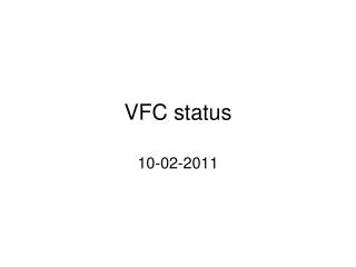
VFC status. 10-02-2011. -The test set-up- SW and Simulation. S-FPGA code. Python test Routines and Board ‘Driver’. VME master model. VFC model. A-FPGA code. Verilog simulation. Linux PC. -The test set-up- SW and HW. S-FPGA code. Python test Routines and Board ‘Driver’.

E N D
VFC status 10-02-2011
-The test set-up-SW and Simulation S-FPGA code Python test Routines and Board ‘Driver’ VME master model VFC model A-FPGA code Verilog simulation Linux PC
-The test set-up-SW and HW S-FPGA code Python test Routines and Board ‘Driver’ VMEio Library A-FPGA code MEN A20 VFC VME crate
What we can do today • The boards can be accessed via VME • The System FPGA can be programmed via the PROM at power up • The communication between the System and the Application FPGAs is implemented using the slow (4 *100Mbps) bus • The 2 SRAMS are working at least up to 100MHz • It is possible to control the VADJ1 between 1.2 and 3.3V from the S-FPGA using the dedicated digital potentiometer • The front panel lemo connection are all working
What remains to be tested • PLLs, Voltage monitoring ADC, VCTXO DAC (Interfaces available, working on the SW) • SiLab XO (reprogramming) • 1-wire unique ID and temperature monitoring • GBit interfaces • DDS (configuration interface available) • DDR3 • Rear Transition Module (P2) and FMCs connection bandwidth
Identified bugs • Inverted polarity on the LVDS output of the DDS (180 degree phase shift) • The direction pin on the LVDS and TTL buffer cannot be controlled (requires manual soldering resulting in a fixed direction) • Wrong name on the schematic for 2 signals • The swing of the VCTXO from Rakon is too smallPossible solder problem on some VME buffers due to the layout
What we might want to change • The SRAMs for QDRs • Do we want to keep the P0?
Available HW • 2 working VFC • 10 VFC ordered