Data Converter Performance Metric
Data Converter Performance Metric. EE174 – SJSU Tan Nguyen. Typical Sampling Process C.T. S.D. D.T. Analog-to-Digital Converter (ADC).

Data Converter Performance Metric
E N D
Presentation Transcript
Data Converter Performance Metric EE174 – SJSU Tan Nguyen
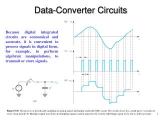
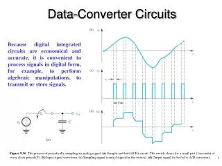
Analog-to-Digital Converter (ADC) The theoretical ideal transfer function for an ADC is a straight line; however, the practical ideal transfer function is a uniform staircase characteristic shown in Figure 1. An ideal ADC uniquely represents all analog inputs within a certain range by a limited number of digital output codes. Each digital code represents a fraction of the total analog input range. Since the analog scale is continuous, while the digital codes are discrete, there is a quantization process that introduces an error. As the number of discrete codes increases, the corresponding step width gets smaller and the transfer function approaches an ideal straight line. The steps are designed to have transitions such that the midpoint of each step corresponds to the point on this ideal line.
Analog-to-Digital Converter (ADC) The width of one step is defined as 1 LSB. It is also a measure of the resolution of the converter since it defines the number of divisions or units of the full analog range. Hence, 1/2 LSB represents an analog quantity equal to one half of the analog resolution. The resolution of an ADC is usually expressed as the number of bits in its digital output code. For example, an ADC with an n-bit resolution has 2n possible digital codes which define 2n step levels. However, since the first (zero) step and the last step are only one half of a full width, the full-scale range (FSR) is divided into 2n-1step widths. Hence 1 LSB = FSR / (2n– 1) for an n-bit converter
Digital-to-Analog Converter (DAC) The theoretical ideal transfer function for a DAC is also a straight line with an infinite number of steps but practically it is a server of points that fall on the ideal straight line as shown in Figure 2. A DAC represents a limited number of discrete digital input codes by a corresponding number of discrete analog output values. Therefore, the transfer function of a DAC is a series of discrete points as shown in Figure 2. For a DAC, 1 LSB corresponds to the height of a step between successive analog outputs, with the value defined in the same way as for the ADC. A DAC can be thought of as a digitally controlled potentiometer whose output is a fraction of the full scale analog voltage determined by the digital input code.
Static Errors on Converters • Static errors affect the accuracy of the converter when it is converting static (dc) signals. • Each can be expressed in LSB units or a percentage of the FSR. For example, an error of ½ LSB for an 8-bit converter corresponds to 0.2% FSR. • Offset error • Gain error • Integral nonlinearity (INL) • Differential nonlinearity (DNL)
Offset Error (Zero scale error) The offset error is defined as the difference between the nominal and actual offset points.
Gain Error The gain error is defined as the difference between the nominal and actual gain points on the transfer function after the offset error has been corrected to zero.
Differential Nonlinearity (DNL) Error • The differential nonlinearity error is the difference between an actual step width (for an ADC) or step height (for a DAC) and the ideal value of 1 LSB. Therefore if the step width or height is exactly 1 LSB, then the differential nonlinearity error is zero. • If the DNL exceeds 1 LSB, there is a possibility that the converter can become nonmonotonic. This means that the magnitude of the output gets smaller for an increase in the magnitude of the input. In an ADC there is also a possibility that there can be missing codes i.e., one or more of the possible 2nbinary codes are never output.
Best straight-line and end-point fit are two possible ways to define the linearity characteristic of an ADC
Integral Nonlinearity (INL) Error • The integral nonlinearity error is the deviation of the values on the actual transfer function from a straight line. This straight line can be either a best straight line which is drawn so as to minimize these deviations or it can be a line drawn between the end points of the transfer function once the gain and offset errors have been nullified. The second method is called end-point linearity and is the usual definition adopted since it can be verified more directly. • For an ADC the deviations are measured at the transitions from one step to the next, and for the DAC they are measured at each step.
Total Error • The absolute accuracy or total error of an ADC is the maximum value of the difference between an analog value and the ideal midstep value. It includes offset, gain, and integral linearity errors and also the quantization error in the case of an ADC.
AC (or Dynamic) Errors • An ADC's performance has different important specifications when the input varies quickly. These different parameters which define the ADC performance with Dynamic input are mostly specified using single input frequency. The ADC output array is processed using FFT and analyzed for dynamic specifications. • Total Harmonic Distortion (THD) • Signal-to-Noise Ratio (SNR) • Signal-to-Noise and Distortion (SINAD) • Spurious Free Dynamic Range (SFDR) • Conversion Between Units
Differential Non Linearity (DNL) Also referred as Differential Linearity Error, describes deviation between ideal step-size to actual step-size observed for each ADC code. The ideal step-size is 1 LSB. A typical DNL curve is as shown in Figure 4. DNL value is usually specified using one of the following units: LSB or %FSV We can use the same equations explained in Offset and Gain Error sections to convert from LSB to %FSV. For the above ADC, 3 LSB error = 0.0046% FSV
Integral Non Linearity (INL) Also referred as Integral Linearity Error, describes the deviation of the actual transfer function with respect to ideal transfer function for an ADC. By definition, INL for a particular code is the summation of DNL array till that code. A typical INL curve is as shown in Figure 5. INL value is usually specified using one of the following units: LSB or %FSR. The equations explained in Offset Error and Gain Error sections can be used to convert between LSB to %FSV. For the example ADC, 3 LSB error = 0.0046% FSV.
AC (or Dynamic) Errors An ADC's performance has different important specifications when the input varies quickly. The ADC output array is processed using FFT and analyzed for dynamic specifications. Each specification is usually associated with input signal specs in terms of frequency and amplitude. A typical ADC output spectrum plot is shown in Figure 6.
Total Harmonic Distortion (THD) The Total Harmonic Distortion (THD) specification provides information regarding the harmonic energy present in the frequency spectrum for a particular input frequency. The frequency spectrum is typically shown till the Nyquist frequency and the THD calculation usually takes into account all the harmonics energy till Nyquist. Harmonics beyond Nyquist fall back into the frequency spectrum as noise or spurious tone. These are taken care of in the SNR and SINAD specifications. The parameter is usually specified in terms of dB or %. THD = Summation of harmonic energy / Fundamental input energy
Signal-to-Noise Ratio (SNR) The Signal-to-Noise Ratio (SNR) specification provides information regarding the noise energy excluding the fundamental and harmonic energy present in the frequency spectrum for a particular input frequency. The SNR calculation usually integrates noise till Nyquist frequency. If not, the specifications will imply the band of frequency where the noise is integrated. The parameter is usually specified in terms of dB, Vrms, or %. SNR = Fundamental input energy / Summation of noise energy
Signal-to-Noise and Distortion (SINAD) The Signal-to-Noise and Distortion (SINAD) specification provides information regarding the noise and harmonic energy present in the frequency spectrum. The parameter is usually specified in terms of dB, Vrms, or %. SINAD = Fundamental input energy / Summation of noise + distortion energy Spurious Free Dynamic Range (SFDR) The Spurious Free Dynamic Range (SFDR) specification provides information regarding the difference between maximum amplitude tone in frequency spectrum and the fundamental input tone. The parameter is usually defined in dB. SFDR = Fundamental input energy – Max (all frequency bins except fundamental)
Conversion Between Units • Percentage to dB – dB = 20 × log ( Percentage / 100) – that is, 1% = –40 dB and 0.1% = –60 dB • dB to Vrms – Assuming input amplitude as 1 Vrms and for 60 dB SNR, – Noise Amplitude is dB = 20 × log (Input Amplitude / Noise Amplitude) – Noise Amplitude Vrms = 0.001, that is, 1 mVrms – If the spec is –60 dB, then the formula will be dB = 20 × log (Noise Amplitude / Input Amplitude)
THE MATHEMATICAL RELATIONSHIPS BETWEEN SINAD, SNR AND THD There is a mathematical relationship between SINAD, SNR, and THD (assuming all are measured with the same input signal amplitude and frequency. In the following equations, SNR, THD, and SINAD are expressed in dB, and are derived from the actual numerical ratios S/N, S/D, and S/(N+D) as shown below:
Offset Error Example Offset Error value is usually specified using one of the following units: Volts, Least Significant Bits (LSB), %Full Scale Value (%FSV), and parts per million (ppm). For the above example, you can convert between different units as shown in the following example. Calculate a 3 LSB offset error conversion to Volts: Offset Error (V) = Error in LSB × Maximum Input / (2N) Offset Error (V) = 3 × 5 V / (216) FSV = 5V, N=16 Offset Error (V) = 0.000229, that is, 229 μV spacer Offset Error (%FSV) = Offset Error (V) × 100 / Full scale value Offset Error (%FSV) = 0.00458% in term of ppm, with regard to full scale voltage, is Offset Error (ppm FSV) = 46 ppm Though the offset error is usually specified at 25°C in the data sheets, the offset does vary with temperature. The variation in offset is specified as Offset Drift and denoted as ppm/°C. The actual offset at any temperature can be calculated by adding the drift to offset value calculated for room temperature. For the above example if the drift is specified as 1 ppm/°C of REF V. Offset at 85°C = 229 μV + [(85 – 25) × 5 μV] = 529 μV.
Gain Error Example • For the above ADC, if the gain error is 4 LSB, then it can be converted to Volts as follows: • • Gain Error (Volts) = Error in LSB × Maximum Input / (2N) • • Gain Error (Volts) = 4 × 5 / (216) = 0.000305 V, that is, 305 μV • This means the ADC will reach 0xFFFF code for input voltage of 4.999656 V. • If the gain error is –4 LSB, then the device will reach 0xFFFF code for input voltage 5.000267 V. • • Gain Error (%FSV) = Gain Error (V) × 100 / Full scale value • • Gain Error (%FSV) = 0.0061% • Similar to offset error, the gain error is usually specified at 25°C in the data sheets and the gain also varies with temperature. The variation in gain is specified as Gain Drift and denoted as ppm/°C. The actual gain error at any temperature can be calculated by adding the drift to gain error value calculated for room temperature. • For the above example, if the drift is specified as 1 ppm/°C of REF V. • Gain Error at 85°C = 305 μV + [(85 – 25) × 5 μV] = 605 μV.
Total Unadjusted Error (TUE) The Total Unadjusted Error (TUE) specification is an indication of the ADC’s worst rms error without applying any Offset or Gain Error correction. The TUE number is not calculated as a summation of Offset, Gain, DNL and INL errors. Since it is an RMS number, the TUE is calculated as TUE = sqrt (sq(Offset Error) + sq(Gain Error) + sq(DNL) + sq(INL)) It is important to convert all the errors to same units. For example, ADC with Offset Error = 3 LSB, Gain Error = 4 LSB, DNL = 1 LSB and INL = 2 LSB, will have TUE = sqrt (9 + 16 + 1 + 4) and TUE = 5.48 LSB Since the offset and gain error can be calibrated out from the ADC transfer curve, the actual error in the application will be dominated by INL and DNL errors.
High Speed DAC Performance • The ac specifications in evaluating high speed DACs: • Settling time • Glitch impulse area • Distortion • Spurious free dynamic range (SFDR) • Signal-to-noise ratio (SNR)
DAC SETTLING TIME – Full-Scale • Full-scale settling time is the amount of time required for the output to settle with the specified error band measured with respect to the 50% point of either the data strobe to the DAC (if it has a parallel register driving the DAC switches) or the time when the input data to the switches changes (if there is no internal register). • The error band is usually defined in terms of an LSB or % full-scale.
DAC SETTLING TIME Mid-Scale Mid-scale settling time is also of interest, because in a binary-weighted DAC, the transition between the 0111…1 code and the 1000…0 code produces the largest transient. In fact, if there is significant bit skew, the transient amplitude can approach full-scale.
GLITCH IMPULSE AREA Ideally, when a DAC output changes it should move from one value to its new one monotonically. In practice, the output is likely to overshoot, undershoot, or both. This uncontrolled movement of the DAC output during a transition is known as a glitch.
DAC DISTORTION Waveform reconstructed by a DAC from digital data will produce the expected spectrum as well as noise and distortion products. For instance, the mid-scale glitch occurs twice during a single cycle of a reconstructed sinewave (at each mid-scale crossing), and will therefore produce a second harmonic of the sinewave, as shown in Figure 4. Note that the higher order harmonics of the sinewave, which also alias back into the Nyquist bandwidth (dc to fc/2), cannot be filtered.
References: www.ti.com/lit/an/slaa587/slaa587.pdf 1. Understanding Data Converters – SLAA013 2. ADS8318 data sheet – SLAS568A http://www.analog.com/static/imported-files/tutorials/MT-003.pdf http://www.hit.bme.hu/~papay/edu/Acrobat/DataConv.pdf Evaluating High Speed DAC Performance by Walt Kester – Analog Devices MT-013 Tutorial