Understanding Analog-to-Digital and Digital-to-Analog Conversion Techniques
This article delves into the operation of digital integrated circuits, emphasizing the efficiency of processing signals in digital form. It describes the sampling process of analog signals and the functionalities of Analog-to-Digital (A/D) and Digital-to-Analog (D/A) converters. The text covers circuit blocks like binary-weighted registers and R-2R ladders, detailing practical implementations in circuits. The workings of various A/D converter types, including feedback-type, dual-slope, and charge-redistribution methods, are explored, highlighting their significance in modern electronics.

Understanding Analog-to-Digital and Digital-to-Analog Conversion Techniques
E N D
Presentation Transcript
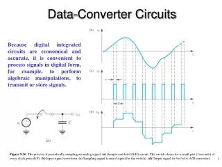
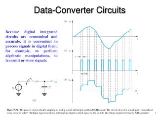
Data-Converter Circuits Because digital integrated circuits are economical and accurate, it is convenient to process signals in digital form, for example, to perform algebraic manipulations, to transmit or store signals. Figure 9.36 The process of periodically sampling an analog signal. (a) Sample-and-hold (S/H) circuit. The switch closes for a small part (t seconds) of every clock period (T). (b) Input signal waveform. (c) Sampling signal (control signal for the switch). (d) Output signal (to be fed to A/D converter).
Analog-to-Digital (A/D) and Digital-to-Analog (D/A) Converters as Functional Blocks Figure 9.37 The A/D and D/A converters as circuit blocks.
D/A Converter Circuits • Binary-weighted registers Figure 9.39 An N-bit D/A converter using a binary-weighted resistive ladder network.
R-2R ladders Figure 9.40 The basic circuit configuration of a DAC utilizing an R-2R ladder network.
Figure 9.41 A practical circuit implementation of a DAC utilizing an R-2R ladder network.
Figure 9.42 Circuit implementation of switch Sm in the DAC of Fig. 9.41. In a BiCMOS technology, Qms and Qmr can be implemented using MOSFETs, thus avoiding the inaccuracy caused by the base current of BJTs.
A/D Converter Circuits • Feedback-type converter Figure 9.43 A simple feedback-type A/D converter.
Dual-slope converter Figure 9.44 The dual-slope A/D conversion method. Note that vA is assumed to be negative.
Parallel converter Figure 9.45 Parallel, simultaneous, or flash A/D conversion.
Charge-redistribution converter • Sample phase • Hold phase • Redistribution phase 01101 Figure 9.46 Charge-redistribution A/D converter suitable for CMOS implementation: (a) sample phase, (b) hold phase, and (c) charge-redistribution phase.