Download
1 / 1
10 likes | 124 Vues
Photoemission by M ulti-photon Absorption from Bulk GaAs. E . Brunkow 1 , N. B. Clayburn 1 , M. LeDoux 2 , and T. J. Gay 1 1 Department of Physics and Astronomy, University of Nebraska, Lincoln, NE 68588-0299 2 Department of Physics, Western Washington University, Bellingham, WA 98225.

E N D
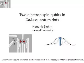
Photoemission by Multi-photon Absorption from Bulk GaAs • E. Brunkow1, N. B. Clayburn1, M. LeDoux2, and T. J. Gay1 1 Department of Physics and Astronomy, University of Nebraska, Lincoln, NE 68588-0299 2 Department of Physics, Western Washington University, Bellingham, WA 98225 Introduction Multi-photon Absorption Results The state-of-the-art source of polarized electrons – photoemission from negative electron affinity (NEA) GaAs – is based on difficult technology [1]. We propose a new polarized electron source, using multi-photon absorption without the need of NEA. We present results that show photoemission can occur without the benefit of a NEA surface. The proposed multi-photon absorption process uses a femtosecond laser pulse to optically pump electrons and impart enough energy to them so they can surmount the crystal’s work function (band gap + electron affinity). The first photon excites the electron from the ground state to the state in the conduction band. A second photon excites the electron from the s state to a virtual state. The electron will absorb two additional photons, the first exciting the electron to a second virtual state, and the second causing the electron to be photo-emitted (Fig 2). The lifetimes of these virtual states are much longer than the femtosecond pulse. Using a KM-Labs Griffin oscillator operating at an average output power up to 100 mW, we have studied the photo-emitted current from bulk GaAs (Fig 3). In these studies, the Griffin pulses of ~ 10 nJwith a repetition rate of 100 MHz were focused to a spot size diameter of ~ 100 μm at the surface of the GaAs crystal. We observed count rates up to 1 kHz as measured by a channel electron multiplier. The extracted electron current obeyed a power law that scaled as the peak pulse intensity to the 4.06 ± 0.085 (Fig 4). At present, the measured currents are orders of magnitude below those required for a useful source. Active efforts to increase the current yield are being made. Negative Electron Affinity In bulk GaAs, the vacuum level is 4.07 eV above the conduction band. This prevents electrons in the valence band from being ejected from the bulk by a single photon of λ ≈ 800 nm, the wavelength necessary to excite an electron to the conduction band. Application of layers of cesium and oxygen to GaAs that has been atomically cleaned can lower the vacuum level below that of the conduction band, resulting in NEA (Fig 1). This in turn allows for an ~ 800 nm continuous wave laser to photo-emit electrons. Fig. 2. Four photon ionization of GaAs. The first photon excites the electron to the conduction band. The second and third photons excite the electron to virtual states. The fourth photon causes the electron to be photo-emitted into the vacuum. Fig. 4. Measurement of electron photoemission from GaAs induced by femtosecond laser pulses. References Fig. 1.Energy bands of p-type GaAs. a) Bulk GaAs with Eg = 1.42 eV and an electron affinity of 4.07 eV. b) GaAs with a Cs layer deposited on the surface of the crystal. c) NEA GaAs generated by applying Cs and O2 layers to the surface which lowers the vacuum level below the conduction band energy. [1] D.T. Pierce et al., Appl. Phys. Lett. 26, 670 (1975). [2] D.T. Pierce and F. Meier, Phys. Rev. B 13, 5484 (1976). Funding: NSF PHY-1206067, Fig. 3. Optical system used to generate femtosecond laser pulses.