Download
1 / 15
150 likes | 375 Vues
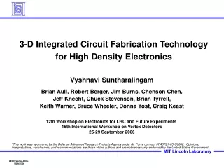
Abstract: 3-D integrated circuits have unique fabrication designs that makes it inexpensive, compact, and more efficient than planar circuits. The components are integrated vertically and horizontally using less material. 3-D IC Fabrication and Devices. Mai Chery Vue and Dylan Scheunemann

E N D
Abstract: 3-D integrated circuits have unique fabrication designs that makes it inexpensive, compact, and more efficient than planar circuits. The components are integrated vertically and horizontally using less material. 3-D IC Fabrication and Devices Mai Chery Vue and Dylan Scheunemann Wednesday April 23, 2014
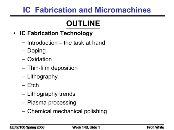
Outline • Fabrication • Types • Monolithic • Wafer-on-Wafer • Die-on-Wafer • Die-on-Die • Wafer-on-Wafer Steps • Advantages/Disadvantages • Applications
Introduction to 3-D IC’s • A Single Circuit with two or more layers of active components. • Components can be integrated both vertically and horizontally.
3-D IC Stacked Problem with stacking is heat dissipation.
Types of Fabrication • Monolithic • Built on single wafer. • Diced into 3-D IC’s. • Wafer-on-Wafer • Built on two or more wafers. • Aligned, bonded, and diced into 3-D IC’s. • Die-On-Wafer • Components built on two wafers. • One wafer diced and aligned on the second wafer. • Die-On-Die • Components built on multiple dice. • Aligned and bonded into 3-D IC’s.
Types of Fabrication Chip means Die
Fabrication (Wafer-on-Wafer) • Components are built on two or more wafers • Alignment of wafers • Machine checks for alignment mark • Temporarily brought into contact • Inspected for correct alignment • Bonding of wafers • Then bonded together using the method best suited for that wafer • Such as Direct, Adhesive, or Thermocompression bonding
Fabrication (Wafer-on-Wafer) • Thinning of wafers • Can be thinned before or after bonding • Dicing Before Grinding • Saws the front before thinning from the back • Dicing By Thinning • Applies a trench-etching process • Reduces Damage
Fabrication (Wafer-on-Wafer) • Dicing of wafers • Scribe and Break • Mechanical Sawing • Laser Cutting
Advantages • Chip Performance • Higher Bandwidth • Reduced Power Consumption • Functionality • Circuit Security • Device Packing Density • Fits into a small space • Shorter Interconnects • Cheaper fabrication costs
Disadvantages • Heat due to stacking • Testing methods • Interconnect design • CAD algorithms and tools
Applications • Monolithic IC 3D (Company in California) • FPGA, Gate Array • DRAM • NAND Flash Memory • Image Sensors • Microdisplays
Summary 3-D integrated circuits have layered active components that are vertically and horizontally integrated. With these designs, there’s about four different fabrication types: monolithic, wafer-on-wafer, die-on-wafer, and die-on-die. These new fabrication designs provide for better chip performance, circuit security, smaller interconnects, and inexpensive circuits.
References Information: • http://domino.research.ibm.com/tchjr/journalindex.nsf/9fe6a820aae67ad785256547004d8af0/2f263eb510ba6030852571c500032694!OpenDocument • http://en.wikipedia.org/wiki/Three-dimensional_integrated_circuit • http://homepages.rpi.edu/~luj/Papers/Luj4.pdf • http://www.wiley-vch.de/publish/dt/books/newTitles201201/3-527-32646-4/?sID=p2qlnooj68su7htl8qrrc2qjt3 • http://electroiq.com/blog/2003/03/wafer-thinning-techniques-for-ultra-thin-wafers/ • https://www.coherent.com/Applications/index.cfm?fuseaction=Forms.page&PageID=273 • http://www.monolithic3d.com/applications.html • Three-Dimensional Integrated Circuit Design by Vasilis F. Pavlidis & Eby G. Friedman • Pictures: • http://esl.epfl.ch/page-42448-en.html • http://lsi.epfl.ch/page-13135-en.html • http://www.intechopen.com/books/metallurgy-advances-in-materials-and-processes/low-temperature-wafer-level-metal-thermo-compression-bonding-technology-for-3d-integration • http://www.tezzaron.com/technology/FaStack.htm
Five Key Concepts • A 3-D circuit is a Single Circuit with two or more layers of active components. • 4 Types of Fabrications • Monolithic, Wafer-on-Wafer, Die-on-Wafer, Die-on-Die • Wafer-on-Wafer Fabrication • Align, Bond, Thin, Dice • Disadvantage: Heat from stacking • Applications: NAND Flash Memory, and Micro Displays