3-D Integrated Circuit Fabrication Technology for High Density Electronics
460 likes | 702 Vues
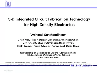
3-D Integrated Circuit Fabrication Technology for High Density Electronics. Vyshnavi Suntharalingam Brian Aull, Robert Berger, Jim Burns, Chenson Chen, Jeff Knecht, Chuck Stevenson, Brian Tyrrell, Keith Warner, Bruce Wheeler, Donna Yost, Craig Keast.

3-D Integrated Circuit Fabrication Technology for High Density Electronics
E N D
Presentation Transcript
3-D Integrated Circuit Fabrication Technology for High Density Electronics Vyshnavi Suntharalingam Brian Aull, Robert Berger, Jim Burns, Chenson Chen, Jeff Knecht, Chuck Stevenson, Brian Tyrrell, Keith Warner, Bruce Wheeler, Donna Yost, Craig Keast 12th Workshop on Electronics for LHC and Future Experiments 15th International Workshop on Vertex Detectors 25-29 September 2006 *This work was sponsored by the Defense Advanced Research Projects Agency under Air Force contract #FA8721-05-C0002. Opinions, interpretations, conclusions, and recommendations are those of the authors and are not necessarily endorsed by the United States Government .
Motivation for 3-D Circuit Technology Process Technology Optimized by Tier • 3-D Circuit = Multi-layer (multi-tier) stacked circuit • Advantages • Reduced interconnect length • Reduced chip size • Reduced parasitics • Reduced power • Fabrication process optimized by tier function • Applications • High bandwidth microprocessors • Mixed material system integration • Advanced focal planes • Local computation and/or memory • 100% fill-factor diodes High Density Vertical Interconnections Bump/Optical Connection Sites Mixed Material System Integration
Pad-Level “3D Integration”Die Stacking Stacked-Die Wire Bonding Stacked Chip-Scale Packages 1 mm ChipPAC, Inc. Tessera, Inc. In Production!
Pixel-Level 3-D IntegrationCross Sections Through Two-Tier Imager 5 mm 8 m Pixel SOI-CMOS (Tier 2) SEM cross section Photodiode (Tier 1) 8 mm decorated Transistor CMOS Vias 3D-Via Bond Interface Diode
Outline Advantages of Vertical Integration for Focal Planes MIT-LL Demonstration of Three-tier ring oscillators Fabrication Sequence MIT Lincoln Laboratory Demonstrations Two-tier backside-illuminated visible imager Three-tier laser radar focal plane Three-tier 3-D IC Multiproject Run Two-tier bonding and interconnection to InP detector material Summary
Limitations – Standard Bulk CMOS APSMonolithic APS – MAPS photodiode OUT RST VDD ROW Pixel Layout • Fill factor compromised • Photodetector and pixel transistors share same area • Low photoresponsivity • Shallow junctions • High doping • Limited depletion depth • High leakage • LOCOS/STI, salicide • Transistor short channel effects • Substrate bounce and transient coupling effects VDD ROW OUT RST n+ p+ Field Oxide n-Well p-well p-epi p+ Substrate
Advantages of Vertical Integration pixel Conventional Monolithic APS 3-D Pixel Light • Pixel electronics and detectors share area • Fill factor loss • Co-optimized fabrication • Control and support electronics placed outside of imaging area PD pixel PD 3T Addressing ROIC Processor Addressing A/D, CDS, … • 100% fill factor detector • Fabrication optimized by layer function • Local image processing • Power and noise management • Scalable to large-area focal planes
Approaches to 3D Integration(Photos Shown to Scale) Tier-1 10 mm 3D-Vias Tier-3 3D-Vias Tier-2 Tier-1 10 mm 10 mm Tier-2 Photo Courtesy of RTI Two-layer stack with insulated vias through thinned bulk Si Bump Bond used to flip-chip interconnect two circuit layers Three-layer circuit using Lincoln’s SOI-based vias
3-Tier, 3D-Integrated Ring Oscillator (DARPA 3DL1 Multiproject Run) 3D Ring Oscillator Cross-Sectional SEM Tier-3: FDSOI CMOS Layer 3D Via Stacked 3D Via 3D Via Tier-2: FDSOI CMOS Layer Transistors 5 mm Tier-1: FDSOI CMOS Layer Stage Delay (ps) 99-Stage Ring Oscillator @1.5V Power Supply (V) • Functional 3-tier, 3D-integrated ring oscillator • Uses all three active transistor layers, 10 levels of metal and experimental stacked 3D-vias • Demonstrates viability of 3D integration process
Outline Advantages of Vertical Integration for Focal Planes Fabrication Sequence and Five Key Elements Low dark current photodiodes Silicon on Insulator (SOI) circuits Low-temperature, wafer-scale oxide-to-oxide bond Precision overlay High-density vertical interconnection MIT Lincoln Laboratory Demonstrations Three-tier ring oscillators Two-tier backside-illuminated visible imager Three-tier laser radar focal plane Three-tier 3-D IC Multiproject Run Two-tier bonding and interconnection to InP detector material Summary
3-D Circuit Integration Flow-1 • Fabricate circuits on SOI wafers • SOI wafers greatly simplify 3D integration • 3-D circuits of two or more active silicon layers can be assembled Wafer-1 can be either Bulk, SOI, or Compound Semiconductor Buried Oxide Handle Silicon Wafer-1 Buried Oxide Wafer-2 Handle Silicon Buried Oxide Wafer-3 Handle Silicon
1. Low Dark Current Photodiodes 90,000 parallel diodes 10,000 diodes (same area) • Photodiode independent of CMOS • High-resistivity substrates • Back-illumination process • Photodiode leakage <0.2nA/cm2 @ 25ºC • Similar results after 3D-stacking Single tier test structure w/guard ring Full thickness wafer
2. Silicon-On-Insulator Circuits • 3.3-V, 350-nm gate length, fully depleted SOI CMOS • Buried oxide • Dielectric isolation • Reduced parasitic capacitances • Enhanced radiation performance • Essential wafer-thinning etch stop 50 nm Si Buried Oxide Silicon Handle Wafer silicided poly gate contact silicon channel Buried Oxide Handle Wafer
3-D Circuit Stacking • Invert, align, and bond Tier 2 to Tier 1 Oxide-Oxide Wafer Bond SOI Handle Wafer CMOS PD High-Resistivity Bulk Wafer
3-D Circuit Stacking • Remove handle silicon from Tier-2 CMOS PD High-Resistivity Bulk Wafer
3. Low Temperature Oxide Layer-to-Layer Bonding IR Image (low-temperature oxide-bonded wafer pair) 150 mm Bonded Wafer-Pair Cross Section Tier-2 metal oxide bond interface 5 mm Tier-1 metal • Deeply scaled 3-D interconnect technology requires robust wafer-to-wafer bonding technology • MIT-LL low temperature oxide bonding process provides • Thin and controllable bondline • Enables use of standard IC high aspect ratio contact etch and plug fill technologies • ~475oC process • Allows for 3-D interconnect to be sintered • Standard, high reliability semiconductor material
4. Precision wafer-to-wafer overlay Mapping microscope Low mag. microscope NIR microscopes Bottom wafer chuck Top wafer chuck 150-mm dia. wafer Low mag. video 6-axis PZT stage Control computer Pre-align plate Laser interferometer controlled XY stage Mapping video • Provide a wafer-to-wafer alignment accuracy compatible with a submicron 3D Via • Tool based on modern IC wafer stepper technology • 0.5 mm 3-sigma overlay demonstrated Control Interface
Repeatability DataMIT-LL Precision Aligner x x x x x x x x x 150-mm wafer-pair (measurement locations) 40 X Offset Data Y Offset Data 30 Total Percent of Die Measured (%) 20 +/- 0.25m 10 0 -1.0 -0.5 0.0 0.5 1.0 Deviation (mm) • Data from five repeated alignments of same wafer pair • Nine die measured per alignment
3D Via Layout Comparison(Based on MIT-LL 180nm FDSOI CMOS rules) With recently developed precision alignment system and via technology Previous capability CMOS Inverter 3D via 2.0 mm 3D via landing pad 2.0 mm 3D via ~1.0 mm 3D via landing pad 5.5 mm Inter-metal via 0.4 mm
Bonded Two Wafer Imager Stack 150-mm Diameter Wafer Pair
Inter-Tier Via Connections • Pattern, etch, and fill 3-D vias • (Additional circuit tiers could be added) Concentric 3-D Via CMOS PD High-Resistivity Bulk Wafer
5. High Density, High Yield, Compact 3D-Via 3D Via Cross-sections • Leverages standard high-yield IC process technology for 3D interconnection • High density plasma oxide etch of via hole • Chemical vapor deposition of tungsten plug • Chemical mechanical planarization (CMP) to form damascene plug Tier-2 Metal CVD-W Plug Bond Interface Tier-1 Metal Circuit Tier-2 M1 W 3D-Via M2 “Donut” Metal M3 Decorated Bond Interface Oxide Bond Tier-1 Landing Pad Circuit Tier-1 Silicon
Thermal Cycle Effects on 3D-Via ChainsThermal Cycle: 300 K/ 77 K/ 300 K 1 Cycle 2 Cycles 3 Cycles 4 Cycles 5 Cycles 6 Cycles 7 Cycles 8 Cycles 9 Cycles 10 Cycles 3D-Via Chain Resistance vs # of 3D Vias and Thermal Cycles 10000 9000 # of cycles 8000 7000 6000 Total Resistance (Ω) 5000 4000 3000 2000 1000 0 0 1000 2000 3000 4000 5000 6000 7000 8000 9000 10000 # of 3D Vias in Series
Back Metal-1 and Back Metal-2 • Deposit and pattern Back Metal-1 • Deposit and CMP ILD • Deposit and pattern Back Metal-2 • Sinter CMOS PD High-Resistivity Bulk Wafer
Completed Back-Illuminated CMOS Imager • Thin photodiode substrate to 50mm • Epoxy bond to quartz CMOS PD Transparent Substrate Light
Outline Advantages of Vertical Integration for Focal Planes Fabrication Sequence MIT Lincoln Laboratory Demonstrations Three-tier ring oscillators Two-tier backside-illuminated visible imager Three-tier laser radar focal plane Three-tier 3-D IC Multiproject Run Two-tier bonding and interconnection to InP detector material Summary
Four-Side Abuttable Goal pixel Foundry Chip 8 mm Tile with Daughter Chip • 3-D CMOS imagers tiled for large-area focal planes • Foundry fabricated daughter chip bump bonded to non-imaging side Tiled Array mechanical mockup
Four-Side AbuttableVertically Integrated Imager 3D-Integrated Tier-1/Tier-2 wafer pair > 1 million 3D interconnects per imager 150 mm Light • Silicon photodetector layer (Tier-1) • Four-side abuttable 1024 x 1024 array of 8mm x 8mm pixels • Address and readout layer (Tier-2) • 3.3 volt FDSOI CMOS layer • Timing, control, and analog-to-digital electronics (Tier-3) • MOSIS fabricated chip bump bonded to detector array • Active-pixel architecture for radiation tolerance 4 x 4 Tiled Array (mock-up)
Design Goals • Four-side abuttable Active Pixel Sensor • 1024 x 1024 array of 8mm x 8mm pixels • 3-D interconnections per pixel • 3.3-V operating voltage • Full digital control and readout at 10 fps
Completed 3D-Stacked ImagerWafer and Die Layout 150-mm wafer 1024 x 1024 n-reset 1024 x 1024 p-reset + cap p-reset p-reset + cap n-reset p-reset, cap, SOI diode Process Monitoring Devices and Circuits 8mm 22 mm
3T Pixel Schematic and Layout 8mm +PDBIAS 3D-Via VDDA 3-D Via 15fF RST ROW RSTLVL VPIX VSS • Design Variations • pFET Reset with 15fF capacitor • nFET Reset with no capacitor
1024 x 1024 Imager Array Architecture 1 1 1 1 Integration Shift Register Row Select Shift Register Column Select From 256 Four Outputs
Preliminary Tier-1-2 3D Imager Test Results • Electrical probe station preliminary imager test result using frontside illumination • Final processing steps will result in unobstructed backside illuminated device 1024 x 1024 Image from FIRST 3D-Integrated Wafer Pair* SOI-CMOS circuit tier (Tier 2) Photodetector tier (Tier 1) *35-mm slide image projected through CMOS-circuit-side of 3D-integrated imager on chip test station Image acquired at 10 frames/sec (Background Subtracted, Pixel Yield > 99.9%, 3.8M transistors) Presented at 2005 ISSCC
Sample Dark Background Panel 1 Panel 2 Panel 3 Panel 4 • Raw image without fixed pattern noise suppression • Dominant yield detractor is row/column drop-outs Four Analog Outputs Open 3D-Vias
Four-Side Abuttable Vertically Integrated Imaging Tile • Wafer-Scale 3D circuit stacking technology • Silicon photodetector tier • SOI-CMOS address and readout tier • Per-pixel 3D interconnections • 1024 x 1024 array of 8 m x 8 m pixels • 100% fill factor • >1 million vertical interconnections per imager Front Illuminated Back Illuminated Presented at 2005 ISSCC
Outline Advantages of Vertical Integration for Focal Planes Fabrication Sequence MIT Lincoln Laboratory Demonstrations Three-tier ring oscillators Two-tier backside-illuminated visible imager Three-tier laser radar focal plane Three-tier 3-D IC Multiproject Run Two-tier bonding and interconnection to InP detector material Summary
Three-Tier Laser Radar Focal Plane Tier-3: 1.5V FDSOI CMOS Tier-2: 3.5V FDSOI CMOS APD APD Tier-1: 30V Avalanche Photodiode VISA APD Pixel Circuit (~250 transistors/pixel) Pseudorandom counter circuit APD drive/sense circuit Avalanche PD 150 mm VISA 3D Stack Cross Section • Based on single-photon-sensitive Geiger-mode avalanche photodiodes • 64 x 64 demonstration circuit (scalable to large imager formats) • Pixel size reduction from 100 mm to 30 mm • Timing resolution reduction from 1 ns to 0.1 ns • 100x reduction in voxel volume Completed Backside-illuminated 3-tier, 3D Laser Radar wafer
Functional 3D-Integrated, 3-Tier Avalanche Photodiode Focal Plane Completed Pixel Cross-Sectional SEM 3D Via Tier-3: 1.5V SOI CMOS Layer Transistors 3D Via Tier-2: 3.5V SOI CMOS Layer 10 mm Tier-1: 30V Back Illuminated APD Layer 10 mm • VISA laser radar focal plane based on single-photon-sensitive Geiger-mode avalanche photodiodes • 64 x 64 format • 50-mm pixel size To-Scale Pixel Layout of Completed 3-tier Laser Radar Focal Plane Tier-3 High-Speed Counter Tier-2 APD Drive/Sense Circuitry Tier-1 Avalanche Photodiode (APD) ~250 transistors/pixel (50 mm x 50 mm) Presented at 2006 ISSCC
64x64 LADAR Focal PlaneFirst Demonstration of 3-Tier Focal Plane • Rudimentary ladar image of 28” long cone with 8-in timing resolution • Timing circuit limited to only 9-bits of its full 12-bit range Pixels 1 mm Complete 3-tier, back-illuminated 64 x 64 APD Laser Radar Orientation of cone image on focal plane Grayscale range image with superimposed contours False color range image
Outline Advantages of Vertical Integration for Focal Planes Fabrication Sequence MIT Lincoln Laboratory Demonstrations Three-tier ring oscillators Two-tier backside-illuminated visible imager Three-tier laser radar focal plane Three-tier 3-D IC Multiproject Run Two-tier bonding and interconnection to InP detector material Summary
3-D IC Multiproject Run Completed (Three 180-nm, 1.5 volt FDSOI CMOS Tiers) Wafer photo of completed tier-1 150-mm-diameter wafer • MIT-LL 3D circuit integration technology • Preliminary 3D design kits developed • Mentor Graphics – MIT-LL, Cadence – NCSU, Thermal Models – CFRDC • Design guide release 11/04, fab start 6/05, 3D-integration complete 3/06 Concepts being explored in run: 3DL1 Participants (Industry, Universities, Laboratories) 33 Designs
Cross-Section of 3-Tier 3D-integrated Circuit (DARPA 3DL1 Multiproject Run) Back Metal Tier-3: Transistor Layer Tier-3: 180-nm, 1.5V FDSOI CMOS 3D-Via Stacked Vias Metal Fill Tier-2: Transistor Layer Oxide Bond Interface 3D-Via Tier-2: 180-nm 1.5V FDSOI CMOS 3D-Via 3-Level Metal Oxide Bond Interface 10 mm Tier-1: Transistor Layer Tier-1: 180-nm, 1.5V FDSOI CMOS 3 FDSOI CMOS Transistor Layers, 10-levels of Metal
3D Technology Improvements(DARPA 3DL1 Multiproject Run) 5 mm 5 mm 5 mm High-Yield on >5000-link Scaled 3D-via Chains • 3D technology enhancements successfully demonstrated in 3DL1 Run • Stacked 3D-vias for electrical and thermal interconnect • 2X reduction in 3D-via size • Improved tier-to-tier overlay Conventional Scaled Stack 3D-vias demonstrated >95% yield on 4800 link chains Stacked 3D-via resistance ~1W Can be used as thermal vias ~0.5 mm 3s Tier-to-Tier Registration 99-Stage Ring Oscillator @1.5V
Silicon to InP Wafer Bonding • Successful demonstration of 3D-bonding of SOI CMOS circuit layer to InP handle wafer • Enables extension of 3D-integration technology to higher density, longer wavelength focal plane detectors • Tight pixel-pitch IR focal planes and APD arrays • InGaAsP (1.06-mm), InGaAs (1.55-mm) Oxide-bonded circuit layer transferred from silicon wafer 150-mm-diameter InP Wafer
Summary • MIT Lincoln Laboratory-developed 3D circuit integration technology has been applied to advanced focal planes and three-tier computational circuits • Successful demonstrations: • Two-tier visible imager: 1024x1024 array of 8mm x 8mm pixels integrated to 100% fill factor photodiodes, backside illuminated • Three-tier ring oscillators in 180-nm gate length technology • Three-tier laser radar focal plane: 64x64 array of Geiger-mode avalanche photodiodes with per-pixel timing and bias circuitry • Three-tier 3-D IC Multiproject Run in 180-nm gate length technology • Two-tier bonding and interconnection to SWIR-sensitive detector materials (InP)